CXL5512M/P
CMOS-CCD 1H Delay Line for NTSC
For the availability of this product, please contact the sales office.
Description
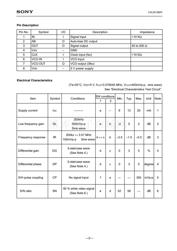
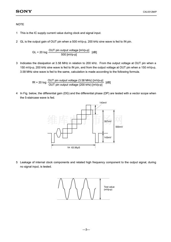
The CXL5512M/P are CMOS-CCD delay line ICs
designed for processing video signals. This ICs
provide a 1H delay time for NTSC signals including
the external lowpass filter.
Features
鈥?/div>
Single 5 V power supply
鈥?/div>
Low power consumption
鈥?/div>
Built-in peripheral circuit
鈥?/div>
Built-in tripling PLL circuit
鈥?/div>
Sync tip clamp mode
Absolute Maximum Ratings
(Ta=25 擄C)
鈥?/div>
Supply voltage
V
DD
+6
鈥?/div>
Operating temperature Topr
鈥?0 to +60
鈥?/div>
Storage temperature Tstg
鈥?5 to +150
鈥?/div>
Allowable power dissipation
P
D
CXL5512M
350
CXL5512P
480
Recommended Operating Range
(Ta=25 藲C)
V
DD
5 V鹵5 %
Recommended Clock Conditions
(Ta=25 藲C)
鈥?/div>
Input clock amplitude V
CLK
400mVp-p (Typ.)
鈥?/div>
Clock frequency
f
CLK
3.579545
MHz
鈥?/div>
Input clock waveform Sine wave
Block Diagram and Pin Configuration
V
DD
VCO OUT
VCO IN
CLK
CXL5512M
8 pin SOP (Plastic)
CXL5512P
8 pin DIP (Plastic)
Input Signal Amplitude
V
SIG
500mVp-p (typ.), 572 mVp-p (max.)
(at internal clamp condition)
Functions
鈥?/div>
680-bit CCD register
鈥?/div>
鈥?/div>
鈥?/div>
鈥?/div>
鈥?/div>
鈥?/div>
Clock driver
Auto-bias circuit
Sync tip clamp circuit
Sample and hold circuit
Tripling PLL circuit
Inverted output
V
擄C
擄C
mW
mW
Structure
CMOS-CCD
8
7
6
5
PLL
Auto-bias circuit
Timing circuit
CCD
(680bit)
Output circuit
(S/H 1 bit)
Clamp circuit
Clock driver
Bias circuit A
Bias circuit B
1
IN
2
AB
3
OUT
4
V
SS
Sony reserves the right to change products and specifications without prior notice. This information does not convey any license by
any implication or otherwise under any patents or other right. Application circuits shown, if any, are typical examples illustrating the
operation of the devices. Sony cannot assume responsibility for any problems arising out of the use of these circuits.
next
CXL5512M/P相關(guān)型號PDF文件下載
-
型號
版本
描述
廠商
下載
-
英文版
CMOS-CCD 1H Delay Line for PAL
-
英文版
CMOS-CCD 1H Delay Line for PAL
SONY [Sony...
-
英文版
CMOS-CCD 1H Delay Line for NTSC
-
英文版
CMOS-CCD 1H Delay Line for NTSC
SONY [Sony...
-
英文版
CMOS-CCD 1H Delay Line for NTSC
-
英文版
CMOS-CCD 1H Delay Line for NTSC
SONY [Sony...
-
英文版
CMOS-CCD 1/2H Delay Line for NTSC
-
英文版
CMOS-CCD 1/2H Delay Line for NTSC
SONY [Sony...
-
英文版
CMOS-CCD 1/2H Delay Line for NTSC
-
英文版
CMOS-CCD 1/2H Delay Line for NTSC
SONY [Sony...
-
英文版
CMOS-CCD 1H Delay Line for PAL
-
英文版
CMOS-CCD 1H Delay Line for PAL
SONY [Sony...
-
英文版
CMOS-CCD 1H Delay Line for PAL
-
英文版
CMOS-CCD 1H Delay Line for PAL
SONY [Sony...
-
英文版
CMOS-CCD 1H Delay Line for NTSC with PLL
-
英文版
CMOS-CCD 1H Delay Line for NTSC with PLL
SONY [Sony...
-
英文版
CMOS-CCD 1H Delay Line for NTSC with PLL
-
英文版
CMOS-CCD 1H Delay Line for NTSC with PLL
SONY [Sony...
-
英文版
CMOS-CCD 1H Delay Line for NTSC
-
英文版
CMOS-CCD 1H Delay Line for NTSC
SONY [Sony...


 1
1
 2
2
 3
3
 4
4
 5
5
 6
6
 7
7
 8
8
 9
9
