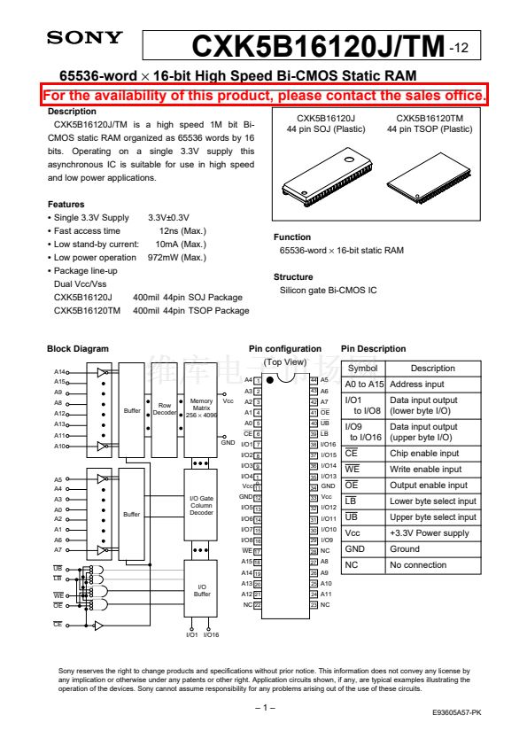
鈥?/div>
Package line-up
Dual Vcc/Vss
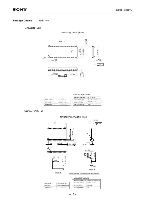
CXK5B16120J
CXK5B16120TM
400mil 44pin SOJ Package
400mil 44pin TSOP Package
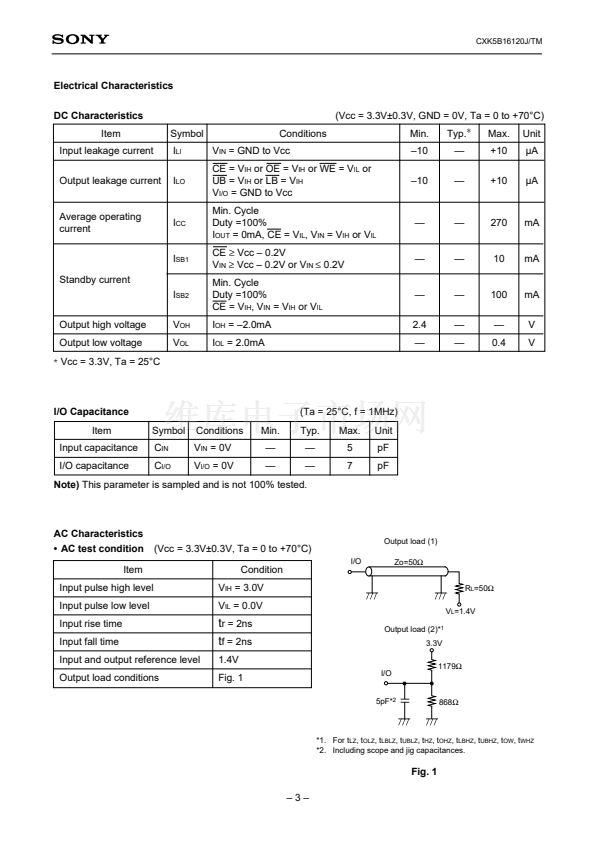
Block Diagram
A14
A15
A9
A8
A12
A13
A11
A10
Buffer
Row
Decoder
Memory
Vcc
Matrix
256
脳
4096
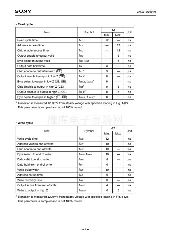
Pin configuration
(Top View)
A4
1
A3
2
A2
3
A1
4
A0
5
CE
6
GND I/O1
7
I/O2
8
I/O3
9
I/O4
1
Vcc
11
I/O Gate
Column
Decoder
GND
12
I/O5
13
I/O6
14
I/O7
15
I/O8
16
WE
17
A15
18
A14
19
I/O
Buffer
A13
20
A12
21
NC
22
0
44
A5
43
A6
42
A7
41
OE
40
UB
39
LB
38
I/O16
37
I/O15
36
I/O14
35
I/O13
34
GND
33
Vcc
32
I/O12
31
I/O11
30
I/O10
29
I/O9
28
NC
27
A8
26
A9
25
A10
24
A11
23
NC
Pin Description
Symbol
Description
A0 to A15 Address input
I/O1
to I/O8
Data input output
(lower byte I/O)
I/O9
Data input output
to I/O16 (upper byte I/O)
CE
WE
OE
LB
UB
Vcc
GND
NC
Chip enable input
Write enable input
Output enable input
Lower byte select input
Upper byte select input
+3.3V Power supply
Ground
No connection
A5
A4
A3
A0
A2
A1
A6
A7
UB
LB
WE
OE
CE
I/O1 I/O16
Buffer
Sony reserves the right to change products and specifications without prior notice. This information does not convey any license by
any implication or otherwise under any patents or other right. Application circuits shown, if any, are typical examples illustrating the
operation of the devices. Sony cannot assume responsibility for any problems arising out of the use of these circuits.
next


 1
1
 2
2
 3
3
 4
4
 5
5
 6
6
 7
7
 8
8
 9
9
 10
10
