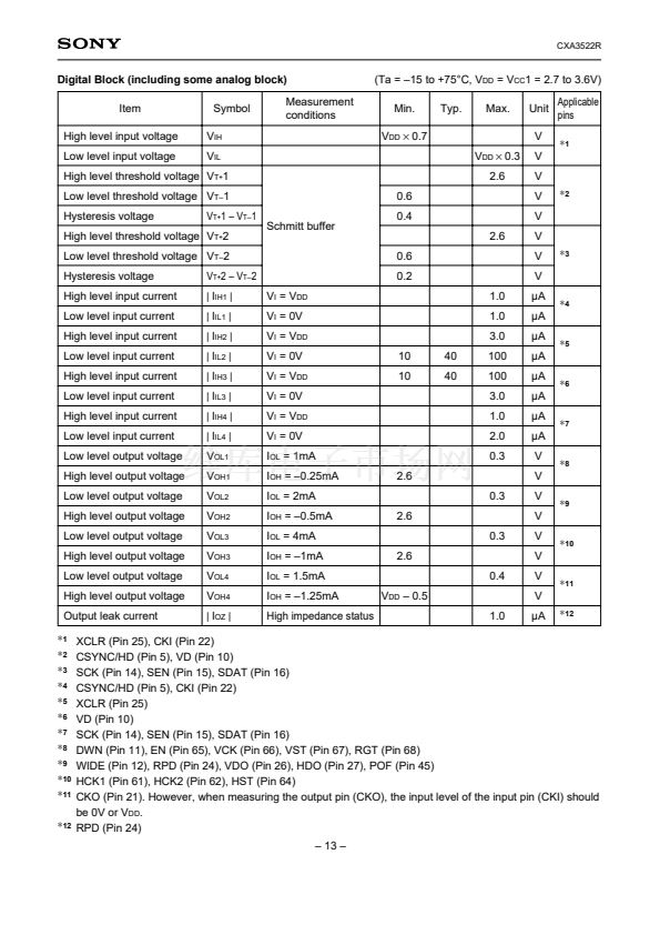
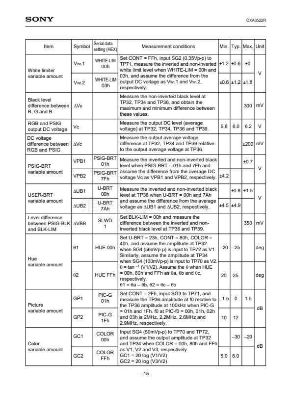
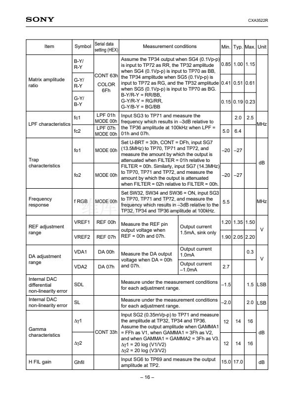
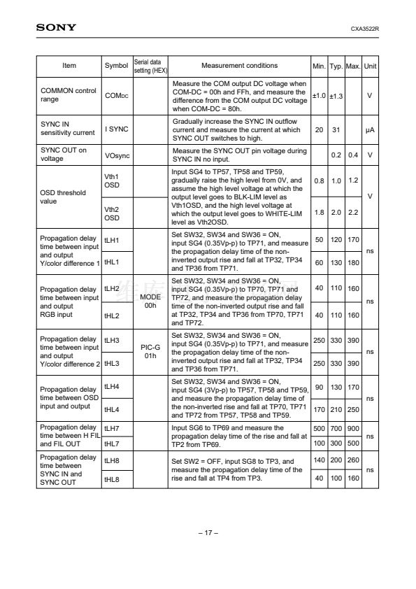
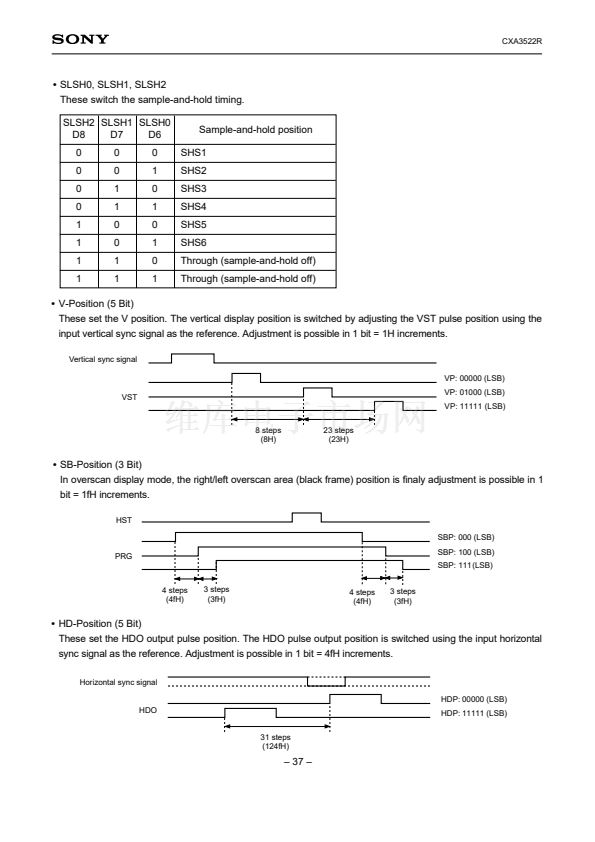
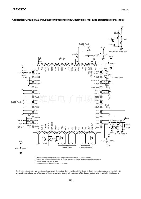
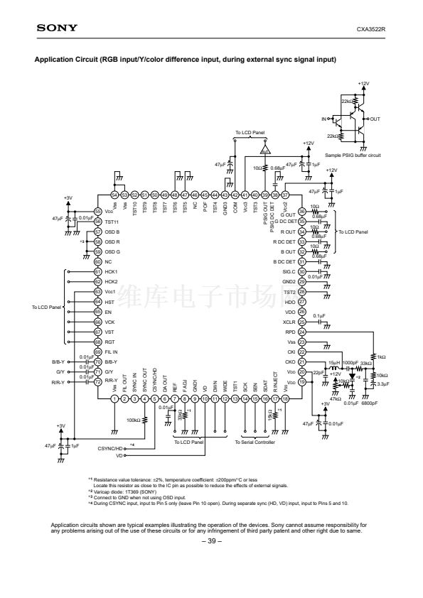
CXA3522R
Driver/Timing Generator for Color LCD Panels
Description
The CXA3522R is an IC designed to drive the color
LCD panel ACX306.
This IC greatly reduces the number of peripheral
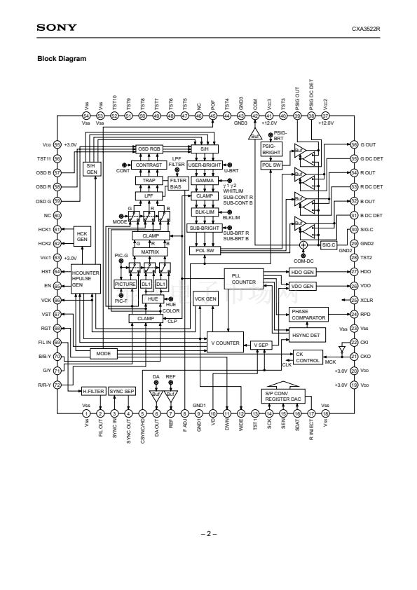
circuits and parts by incorporating a RGB driver and
timing generator for video signals onto a single chip.
This chip has a built-in serial interface circuit and
electronic attenuators which allow various settings to
be performed by microcomputer control, etc.
Features
鈥?/div>
Color LCD panel ACX306 driver
鈥?/div>
Supports NTSC and PAL systems
鈥?/div>
Supports Y/color difference and RGB inputs
鈥?/div>
Supports OSD input (digital input)
鈥?/div>
Power saving function
鈥?/div>
Serial interface circuit
鈥?/div>
Electronic attenuators (D/A converter)
鈥?/div>
Trap and LPF (f0, fc variable)
鈥?/div>
COMMON and PSIG output circuits
鈥?/div>
Sharpness function
鈥?/div>
2-point
緯
correction circuit
鈥?/div>
R, G, B signal delay time adjustment circuit
鈥?/div>
D/A output pin (0 to 3V, 8 level output)
鈥?/div>
Output polarity inversion circuit
鈥?/div>
Supports AC drive for LCD panel during no signal
Applications
Compact LCD monitors, etc.
Absolute Maximum Ratings
(Ta = 25擄C)
鈥?/div>
Supply voltage V
CC
1
6
V
15
V
V
CC
2
V
CC
3
15
V
V
DD
5.5
V
鈥?/div>
Analog input pin voltage
VINA (Pins 57, 58 and 59)
GND 鈥?0.3 to V
CC
1 + 0.3 V
V
VINA (Pins 3, 69)
V
CC
1
VINA (Pin 30)
1.5 to V
CC
2 鈥?4
V
VINA (Pin 71)
0.9
Vp-p
VINA (Pins 70, 72)
0.8
Vp-p
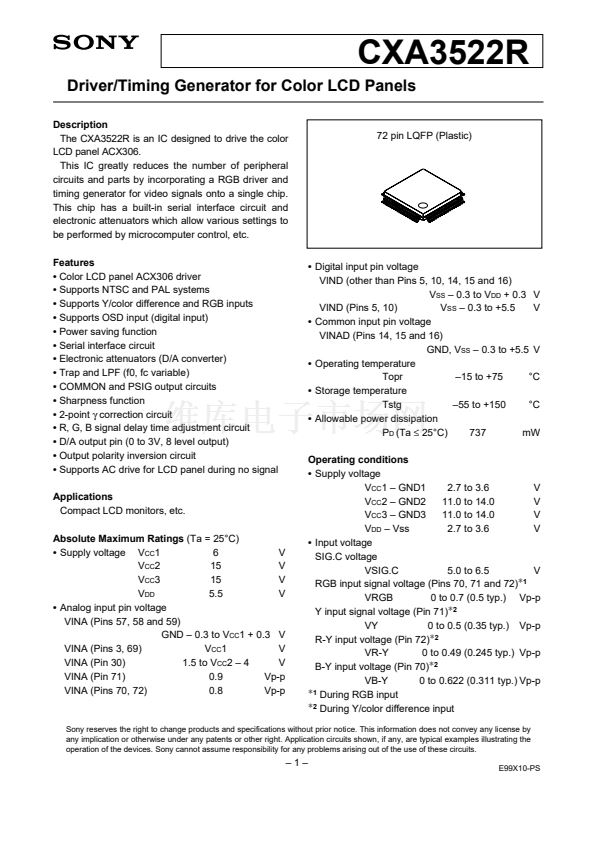
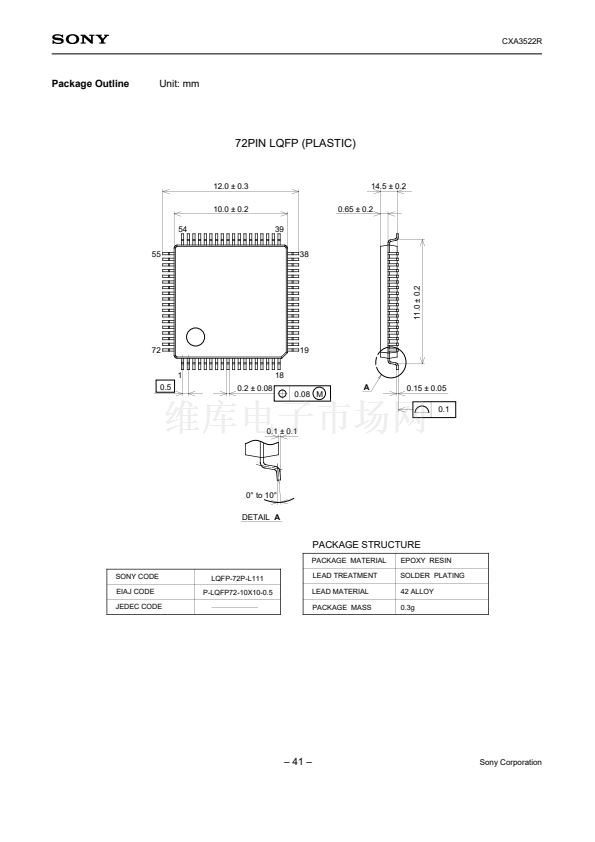
72 pin LQFP (Plastic)
鈥?/div>
Digital input pin voltage
VIND (other than Pins 5, 10, 14, 15 and 16)
V
SS
鈥?0.3 to V
DD
+ 0.3 V
VIND (Pins 5, 10)
V
SS
鈥?0.3 to +5.5
V
鈥?/div>
Common input pin voltage
VINAD (Pins 14, 15 and 16)
GND, V
SS
鈥?0.3 to +5.5 V
鈥?/div>
Operating temperature
Topr
鈥?5 to +75
擄C
鈥?/div>
Storage temperature
Tstg
鈥?5 to +150
擄C
鈥?/div>
Allowable power dissipation
P
D
(Ta
鈮?/div>
25擄C)
737
mW
Operating conditions
鈥?/div>
Supply voltage
V
CC
1 鈥?GND1
2.7 to 3.6
V
V
CC
2 鈥?GND2
11.0 to 14.0
V
V
CC
3 鈥?GND3
11.0 to 14.0
V
V
DD
鈥?Vss
2.7 to 3.6
V
鈥?/div>
Input voltage
SIG.C voltage
VSIG.C
5.0 to 6.5
V
鈭?/div>
1
RGB input signal voltage (Pins 70, 71 and 72)
VRGB
0 to 0.7 (0.5 typ.) Vp-p
Y input signal voltage (Pin 71)
鈭?/div>
2
VY
0 to 0.5 (0.35 typ.) Vp-p
R-Y input voltage (Pin 72)
鈭?/div>
2
VR-Y
0 to 0.49 (0.245 typ.) Vp-p
B-Y input voltage (Pin 70)
鈭?/div>
2
VB-Y
0 to 0.622 (0.311 typ.) Vp-p
鈭?/div>
1
During RGB input
鈭?/div>
2
During Y/color difference input
Sony reserves the right to change products and specifications without prior notice. This information does not convey any license by
any implication or otherwise under any patents or other right. Application circuits shown, if any, are typical examples illustrating the
operation of the devices. Sony cannot assume responsibility for any problems arising out of the use of these circuits.
next
CXA3522R相關(guān)型號PDF文件下載
-
型號
版本
描述
廠商
下載
-
英文版
Read/Write Amplifier (with Built-in Filters) for FDDs
-
英文版
Read/Write Amplifier (with Built-in Filters) for FDDs
SONY [Sony...
-
英文版
8-bit 140MSPS Flash A/D Converter
-
英文版
8-bit 140MSPS Flash A/D Converter
SONY [Sony...
-
英文版
8-bit 120MSPS Flash A/D Converter
SONY [Sony...
-
英文版
NICAM and SMATV RF MODULATOR/PLL
-
英文版
NICAM and SMATV RF MODULATOR/PLL
SONY [Sony...
-
英文版
Wide Band FSK Receiver
-
英文版
Wide Band FSK Receiver
SONY [Sony...
-
英文版
L-band Down Converter for Satellite Tuner
-
英文版
L-band Down Converter for Satellite Tuner
SONY [Sony...
-
英文版
6-bit 140MSPS Flash A/D Converter
-
英文版
6-bit 140MSPS Flash A/D Converter
SONY [Sony...
-
英文版
IF Amplifier for M-ary FSK Pagers
-
英文版
IF Amplifier for M-ary FSK Pagers
SONY [Sony...
-
英文版
IF Amplifier for M-ary FSK Pagers
SONY [Sony...
-
英文版
Achieving Low Power and High Speed in Paging System IF IC
SONY [Sony...
-
英文版
All Band TV Tuner IC with On-chip PLL
-
英文版
All Band TV Tuner IC with On-chip PLL
SONY [Sony...
-
英文版
10-bit 125MSPS D/A Converter


 1
1
 2
2
 3
3
 4
4
 5
5
 6
6
 7
7
 8
8
 9
9
 10
10
 11
11
 12
12
 13
13
 14
14
 15
15
 16
16
 17
17
 18
18
 19
19
 20
20
 21
21
 22
22
 23
23
 24
24
 25
25
 26
26
 27
27
 28
28
 29
29
 30
30
 31
31
 32
32
 33
33
 34
34
 35
35
 36
36
 37
37
 38
38
 39
39
 40
40
 41
41
