CXA3197R
10-bit 125MSPS D/A Converter
Description
The CXA3197R is a high-speed D/A converter
which can perform multiplexed input of two system
10-bit data.
This IC realizes a maximum conversion rate of
125MSPS. Multiplexed operation is possible by
inputing the 1/2 frequency-divided clock or by halving
the frequency of the clock internally with the clock
frequency divider circuit having the reset pin. The
data input is at TTL level, and the clock input and
reset input can select either TTL or PECL level
according to the application.
Features
鈥?/div>
Maximum conversion rate:
During PECL operation: 125MSPS
During TTL operation: 100MSPS
鈥?/div>
Resolution: 10 bits
鈥?/div>
Low power consumption: 480mW (typ.)
鈥?/div>
Data input level: TTL
鈥?/div>
Clock, reset input level: TTL and PECL compatible
鈥?/div>
2:1 multiplexed input function
鈥?/div>
1/2 frequency-divided clock output possible by the
built-in clock frequency divider circuit
鈥?/div>
Voltage output (50鈩?load drive possible)
鈥?/div>
Single power supply or 鹵dual power supply operation
鈥?/div>
Reset signal polarity switching function
AGND2
AOUTP
AOUTN
48 pin LQFP (Plastic)
LEAD TREATMENT: PALLADIUM PLATING
Structure
Bipolar silicon monolithic IC
Applications
鈥?/div>
LCD
鈥?/div>
DDS
鈥?/div>
HDTV
鈥?/div>
Communications (QPSK, QAM)
鈥?/div>
Measuring devices
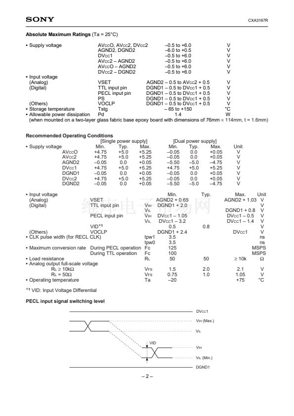
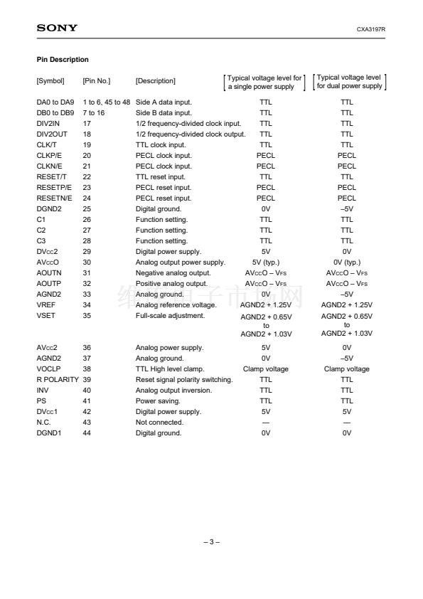
36 35 34 33 32 31 30 29 28 27 26 25
AGND2 37
VOCLP 38
R POLARITY 39
INV 40
PS 41
DV
CC
1 42
N.C. 43
DGND1 44
(MSB) DA9 45
DA8 46
DA7 47
DA6 48
1
2
3
4
5
6
7
8
9 10 11 12
24 RESETN/E
23 RESETP/E
22 RESET/T
21 CLKN/E
20 CLKP/E
19 CLK/T
18
DIV2OUT
C1
DGND2
17 DIV2IN
16 DB0 (LSB)
15 DB1
14 DB2
13 DB3
Pin Configuration
AV
CC
2
VSET
VREF
AV
CC
O
DV
CC
2
C3
DB7
DA3
DA2
DA4
(MSB) DB9
DA5
DB8
DB6
C2
(LSB) DA0
Sony reserves the right to change products and specifications without prior notice. This information does not convey any license by
any implication or otherwise under any patents or other right. Application circuits shown, if any, are typical examples illustrating the
operation of the devices. Sony cannot assume responsibility for any problems arising out of the use of these circuits.
DA1
next
CXA3197R相關(guān)型號PDF文件下載
-
型號
版本
描述
廠商
下載
-
英文版
Read/Write Amplifier (with Built-in Filters) for FDDs
-
英文版
Read/Write Amplifier (with Built-in Filters) for FDDs
SONY [Sony...
-
英文版
8-bit 140MSPS Flash A/D Converter
-
英文版
8-bit 140MSPS Flash A/D Converter
SONY [Sony...
-
英文版
8-bit 120MSPS Flash A/D Converter
SONY [Sony...
-
英文版
NICAM and SMATV RF MODULATOR/PLL
-
英文版
NICAM and SMATV RF MODULATOR/PLL
SONY [Sony...
-
英文版
Wide Band FSK Receiver
-
英文版
Wide Band FSK Receiver
SONY [Sony...
-
英文版
L-band Down Converter for Satellite Tuner
-
英文版
L-band Down Converter for Satellite Tuner
SONY [Sony...
-
英文版
6-bit 140MSPS Flash A/D Converter
-
英文版
6-bit 140MSPS Flash A/D Converter
SONY [Sony...
-
英文版
IF Amplifier for M-ary FSK Pagers
-
英文版
IF Amplifier for M-ary FSK Pagers
SONY [Sony...
-
英文版
IF Amplifier for M-ary FSK Pagers
SONY [Sony...
-
英文版
Achieving Low Power and High Speed in Paging System IF IC
SONY [Sony...
-
英文版
All Band TV Tuner IC with On-chip PLL
-
英文版
All Band TV Tuner IC with On-chip PLL
SONY [Sony...
-
英文版
10-bit 125MSPS D/A Converter


 1
1
 2
2
 3
3
 4
4
 5
5
 6
6
 7
7
 8
8
 9
9
 10
10
 11
11
 12
12
 13
13
 14
14
 15
15
 16
16
 17
17
 18
18
 19
19
 20
20
 21
21
 22
22
 23
23
 24
24
 25
25
 26
26
 27
27
 28
28
 29
29
 30
30
