鈥?/div>
Storage temperature range
Tstg
Operating Conditions
Supply voltage
V
CC
14
鈥?5 to +80
鈥?5 to +150
V
擄C
擄C
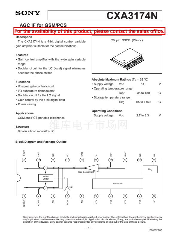
20 pin SSOP (Plastic)
2.7 to 3.3
V
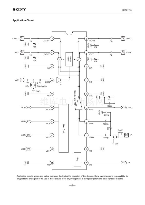
Block Diagram and Package Outline
IXOUT
IOUT
GND
V
CC
IFIN
IFINX
NC
NC
NC
20
19
18
17
16
15
14
13
12
11
Reg
Gain Control AMP
Phase
Shifter
Gain Cont
脳
2
1
QXOUT
2
QOUT
3
NC
4
LOIN
5
NC
6
VC4
7
VC3
8
VC2
9
VC1
10
Sony reserves the right to change products and specifications without prior notice. This information does not convey any license by
any implication or otherwise under any patents or other right. Application circuits shown, if any, are typical examples illustrating the
operation of the devices. Sony cannot assume responsibility for any problems arising out of the use of these circuits.
next


 1
1
 2
2
 3
3
 4
4
 5
5
 6
6
 7
7
 8
8
 9
9
 10
10
