鈥?/div>
Pin voltage
鈥?.3 to V
CC
+ 0.3 V
Operating Conditions
Supply voltage
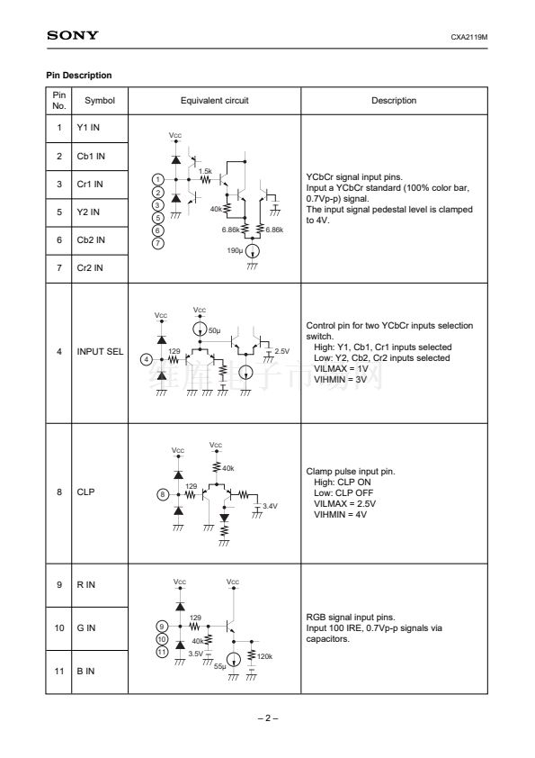
Block Diagram
SIG OUT
SIG2 IN
SIG3 IN
SIG1 IN
Cr OUT
Cb OUT
SEL1
GND
Y OUT
SEL2
V
CC
YM
NC
15
CLP
14
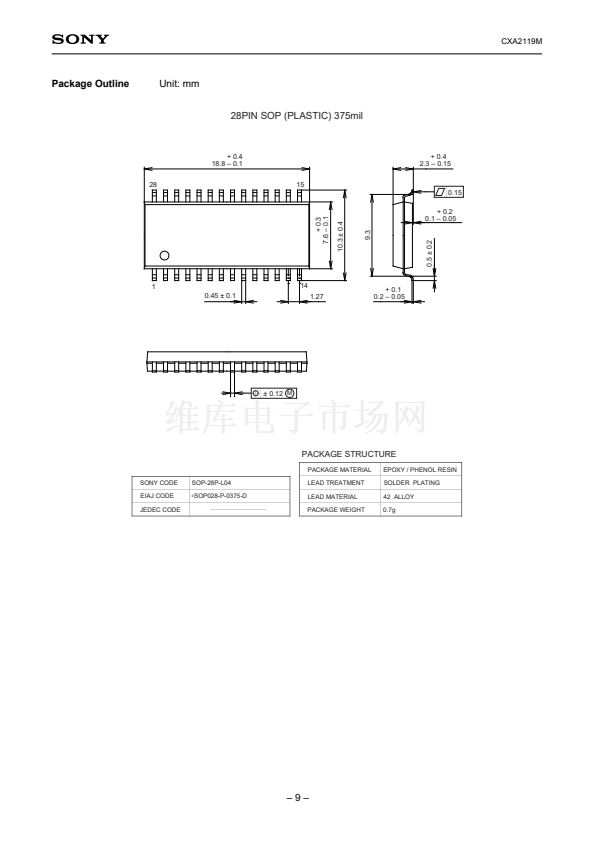
28 pin SOP(Plastic)
Applications
TV
Structure
Bipolar silicon monolithic IC
V
CC
9.0 鹵 0.5
V
YS
28
27
26
25
24
23
22
21
20
19
18
17
16
6dB
0/鈥?dB
SW
6dB
6dB
CLP
6dB
CLP
6dB
CLP
6dB
CLP
6dB
CLP
6dB
CLP
Cr
6dB
6dB
Cb
Y
RGB
YCbCr
MATRIX
CLP
CLP
1
2
3
4
5
6
7
8
9
10
11
12
13
Cb2 IN
Cr1 IN
YCLP
R IN
Cb1 IN
Sony reserves the right to change products and specifications without prior notice. This information does not convey any license by
any implication or otherwise under any patents or other right. Application circuits shown, if any, are typical examples illustrating the
operation of the devices. Sony cannot assume responsibility for any problems arising out of the use of these circuits.
INPUT SEL
鈥?鈥?/div>
CbCLP
CrCLP
E97511-PS
Y2 IN
CLP
Cr2 IN
Y1 IN
G IN
B IN


 1
1
 2
2
 3
3
 4
4
 5
5
 6
6
 7
7
 8
8
 9
9
