鈥?/div>
Dual channels for diversity
+29.5 dBm Input IP3
+12 dBm Input P1dB
RF: 800 鈥?925 MHz
IF: 200 鈥?250 MHz
Single supply operation (+5 V)
6x6 mm 28-pin QFN package
Low-side LO configuration
Common footprint with other
PCS/UMTS/cellular versions
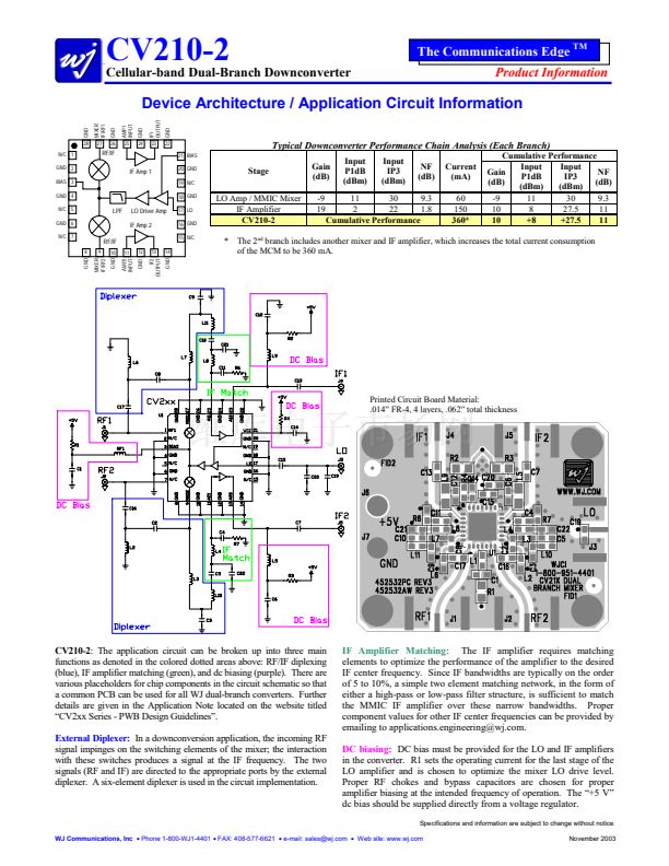
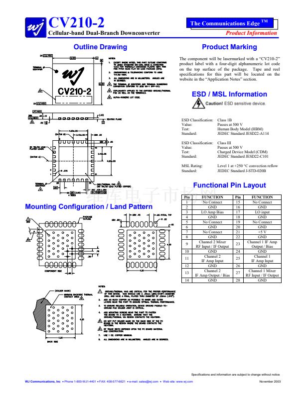
RF/IF
IF Amp 1
GND
22
21 BIAS
20 GND
19 N/C
18 GND
17 LO
16 GND
15 N/C
14
GND
LPF
LO Driver Amp
IF Amp 2
RF/IF
10
GND
11
AMP2
INPUT
12
GND
13
IF2
OUTPUT
Top View
Specifications
1
Parameters
RF Frequency Range
LO Frequency Range
IF Center Frequency Range
% Bandwidth around IF center frequency
SSB Conversion Gain
Gain Drift over Temp (-40擄 C to 85擄 C)
Input IP3
Input IP2
Input 1 dB Compression Point
Noise Figure
LO Input Drive Level
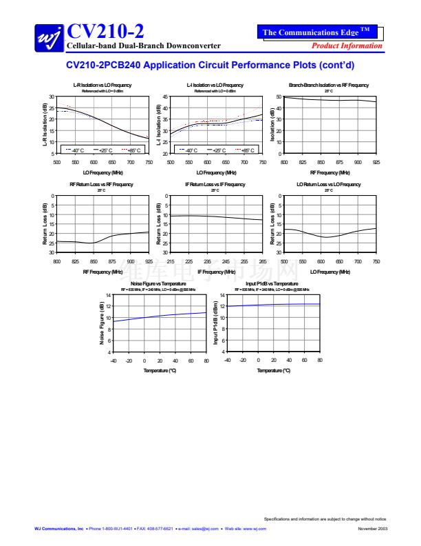
LO-RF Isolation
LO-IF Isolation
Branch-Branch Isolation
Return Loss: RF Port
Return Loss: LO Port
Return Loss: IF Port
Operating Supply Voltage
Supply Current
Thermal Resistance
Junction Temperature
Units
MHz
MHz
MHz
%
dB
dB
dBm
dBm
dBm
dB
dBm
dB
dB
dB
dB
dB
dB
V
mA
擄C / W
擄C
Min
800
550
200
8
-1.5
+25
+33
Typ
Max
925
725
250
12
1.5
Comments
-2.5
320
240
鹵7.5
10
鹵0.3
+29.5
+39
+12
10.2
0
18
32
45
20
20
12
+5
360
See note 2
See note 3
Temp = 25擄 C
Referenced to +25擄 C
See note 4
See note 4
See note 4
See note 5
P
LO
= 0 dBm
P
LO
= 0 dBm
+2.5
475
27
160
See note 6
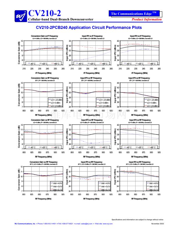
1. Specifications when using the application specific circuit (shown on page 3) with a low side LO = 0 dBm in a downconverting application at 25擄 C.
2. IF matching components affect the center IF frequency. Proper component values for other IF center frequencies than shown can be provided by emailing to applications.engineering@wj.com.
3. The IF bandwidth of the converter is defined as 15% around any center frequency in its operating IF frequency range. The bandwidth is determined with external components. Specifications are valid around
the total 鹵7.5% bandwidth. ie. with a center frequency of 240 MHz, the specifications are valid from 240 鹵 18 MHz.
4. Assumes the supply voltage = +5 V. IIP3 is measured with
鈭唂
= 1 MHz with RF
in
= -5 dBm / tone.
5. Assumes LO injection noise is filtered at the thermal noise floor, -174 dBm/Hz, at the RF, IF, and Image frequencies.
6. The maximum junction temperature ensures a minimum MTBF rating of 1 million hours of usage.
Absolute Maximum Rating
Parameters
Operating Case Temperature
Storage Temperature
DC Voltage
Junction Temperature
Ordering Information
Part No.
CV210-2
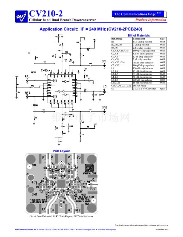
CV210-2PCB240
Rating
-40擄 to +85擄 C
-55擄 to +125擄 C
+5.5 V
+220 擄C
Description
Cellular-band Dual-Branch Downconverter
Fully-Assembled Application Board, IF = 240 MHz
Operation of this device above any of these parameters may cause permanent damage.
Specifications and information are subject to change without notice
WJ Communications, Inc
鈥?/div>
Phone 1-800-WJ1-4401
鈥?/div>
FAX: 408-577-6621
鈥?/div>
e-mail: sales@wj.com
鈥?/div>
Web site: www.wj.com
November 2003


 1
1
 2
2
 3
3
 4
4
 5
5
 6
6
