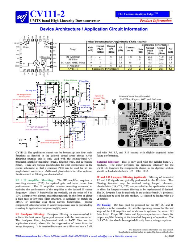
鈥?/div>
RF: 1900 鈥?2200 MHz
IF: 150 鈥?300 MHz
+38 dBm Output IP3
+21 dBm Output P1dB
5 dB Noise Figure
Single supply operation (+5 V)
6x6 mm 28-pin QFN package
Low-side LO configuration
Common footprint with other
PCS/UMTS/cellular versions
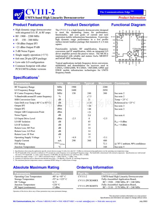
IF
RF Amp
GND
22
21 IF OUT
19 N/C
18 GND
17 BIAS
16 GND
15 LO IN
14
GND
LO Driver Amp
RF
LO
12
GND
13
LO OUT
Specifications
1
Parameters
RF Frequency Range
LO Frequency Range
IF Center Frequency Range
% Bandwidth around IF center frequency
SSB Conversion Gain
Gain Drift over Temp (-40擄 C to 85擄 C)
Output IP3
Output IP2
Output 1dB Compression Point
Noise Figure
LO Input Drive Level
LO-RF Isolation
LO-IF Isolation
Return Loss: RF Port
Return Loss: LO Port
Return Loss: IF Port
Operating Supply Voltage
Supply Current
FIT Rating
Junction Temperature
Units
MHz
MHz
MHz
%
dB
dB
dBm
dBm
dBm
dB
dBm
dB
dB
dB
dB
dB
V
mA
failures
/
1E9 hrs
擄C
Minimum
1900
1600
150
Typical
Maximum Comments
2200
2050
300
-2.5
+4.9
290
240
鹵7.5
21
鹵1.0
+38
+48
+21
5.0
0
45
35
14
14
14
+5
360
See note 2
See note 2
Temp = 25擄 C
Referenced to +25擄 C
See note 3
See note 3
See note 4
+2.5
P
LO
= 0 dBm
P
LO
= 0 dBm
+5.1
480
72.1
160
@ 70
o
C ambient, 90% confidence
See note 5
1. Specifications when using the application specific circuit (shown on page 3) with a low side LO = 0 dBm in a downconverting application over the operating case temperature range.
2. The IF bandwidth of the converter is defined as 15% around any center frequency in its operating IF frequency range. The bandwidth is determined with external components. Specifications are valid around
the total 鹵7.5% bandwidth. ie. with a center frequency of 200 MHz, the specifications are valid from 200 鹵 15 MHz.
3. Assumes the supply voltage = +5 V. OIP3 is measured with
鈭唂
= 1 MHz with IF
out
= 5 dBm / tone.
4. Assumes LO injection noise is filtered at the thermal noise floor, -174 dBm/Hz, at the RF, IF, and Image frequencies.
5. The maximum junction temperature ensures a minimum MTBF rating of 1 million hours of usage.
Absolute Maximum Rating
Parameters
Operating Case Temperature
Storage Temperature
DC Voltage
Junction Temperature
RF Input (continuous)
Ordering Information
Part No.
CV111-2
CV111-2PCB240RX
CV111-2PCB240TX
Rating
-40擄 to +85擄 C
-55擄 to +125擄 C
+6 V
+220 擄C
+2 dBm
Description
UMTS-band High Linearity Downconverter
Fully-Assembled Application Board,
RF = 1920 鈥?1980 MHz, IF = 240 MHz
Fully-Assembled Application Board,
RF = 2110 鈥?2170 MHz, IF = 240 MHz
Operation of this device above any of these parameters may cause permanent damage.
This document contains information on a new product.
Specifications and information are subject to change without notice
WJ Communications, Inc
鈥?/div>
Phone 1-800-WJ1-4401
鈥?/div>
FAX: 408-577-6621
鈥?/div>
e-mail: sales@wj.com
鈥?/div>
Web site: www.wj.com
IF IN
IF Amp
20 GND
July 2003


 1
1
 2
2
 3
3
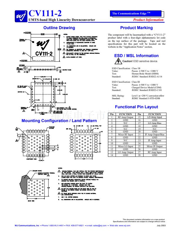 4
4
