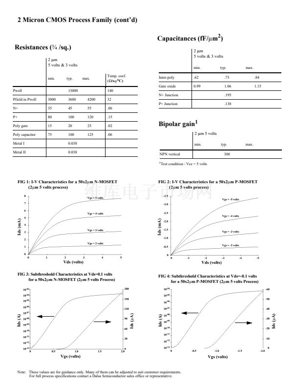
鈥?/div>
150mm Wafers
Description
The 2碌m P-Well process provides flexibility, speed and pack-
ing density needed in mixed signal designs. The aggressive de-
sign rules make it comparable to most 1.5碌m processes. Also,
the MOSFET transistors are designed with very shallow source-
drain junctions and a thin gate oxide to improve speed. A low
voltage option is available for 3 volts applications. It offers low
and matched threshold voltages for improved dynamic range
needed in mixed analog/digital applications.
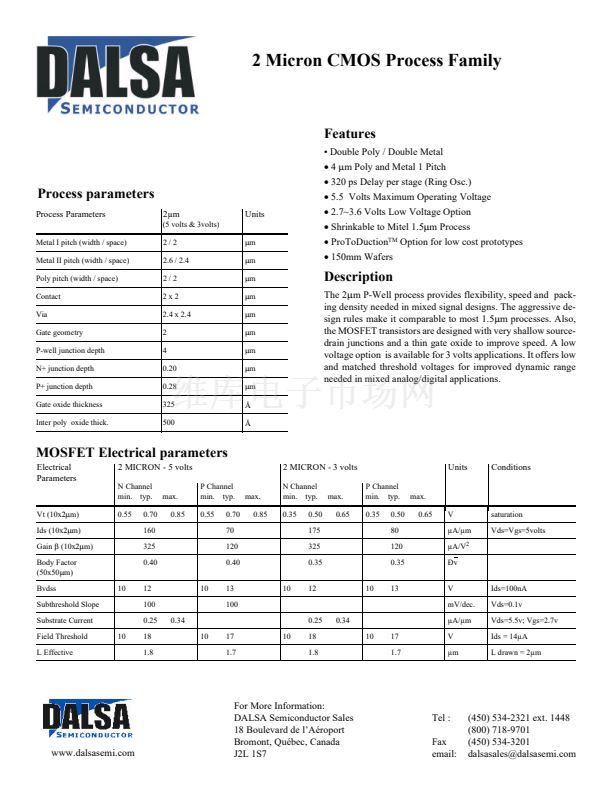
MOSFET Electrical parameters
Electrical
Parameters
2 MICRON - 5 volts
N Channel
min. typ.
Vt (10x2碌m)
Ids (10x2碌m)
Gain
尾
(10x2碌m)
Body Factor
(50x50碌m)
Bvdss
Subthreshold Slope
Substrate Current
Field Threshold
L Effective
10
10
0.55
0.70
160
325
0.40
12
100
0.25
18
1.8
0.34
10
17
1.7
10
10
max.
0.85
P Channel
min. typ.
0.55
0.70
70
120
0.40
13
100
0.25
18
1.8
0.34
10
17
1.7
10
max.
0.85
2 MICRON - 3 volts
N Channel
min. typ.
0.35
0.50
175
325
0.35
12
10
max.
0.65
P Channel
min. typ.
0.35
0.50
80
120
0.35
13
max.
0.65
Units
Conditions
V
碌A(chǔ)/碌m
碌A(chǔ)/V
2
脨v
V
mV/dec.
碌A(chǔ)/碌m
V
碌m
saturation
Vds=Vgs=5volts
Ids=100nA
Vds=0.1v
Vds=5.5v; Vgs=2.7v
Ids = 14碌A(chǔ)
L drawn = 2碌m
www.dalsasemi.com
For More Information:
DALSA Semiconductor Sales
18 Boulevard de l鈥橝茅roport
Bromont, Qu茅bec, Canada
J2L 1S7
Tel :
Fax
email:
(450) 534-2321 ext. 1448
(800) 718-9701
(450) 534-3201
dalsasales@dalsasemi.com


 1
1
 2
2
