鈥?/div>
B
4.06
5.21
C
0.71
0.864
D
2.00
2.72
All Dimensions in mm
C
Maximum Ratings and Electrical Characteristics
Single Phase, half wave, 60Hz, resistive or inductive load.
For capacitive load, derate current by 20%.
@T
A
=25擄C unless otherwise specified
Characteristic
Peak Repetitive Reverse Voltage
Working Peak Reverse Voltage
DC Blocking Voltage
RMS Reverse Voltage
Average Rectified Output Current (Note 1)
@T
A
= 75擄C
Symbol
V
RRM
V
RWM
V
R
V
R(RMS)
I
O
I
FSM
V
FM
I
RM
C
j
R
�JA
T
j
T
STG
BY133
Unit
1300
910
1.0
30
1.0
5.0
50
15
50
-65 to +125
-65 to +150
V
V
A
A
V
碌A
pF
K/W
擄C
擄C
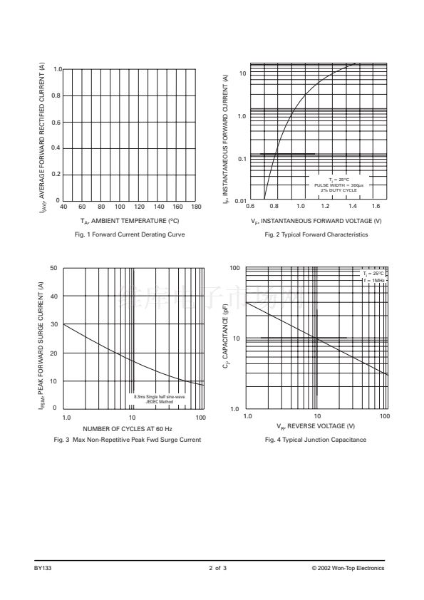
Non-Repetitive Peak Forward Surge Current 8.3ms Single
half sine-wave superimposed on rated load (JEDEC Method)
Forward Voltage
Peak Reverse Current
At Rated DC Blocking Voltage
Typical Junction Capacitance (Note 2)
Typical Thermal Resistance Junction to Ambient (Note 1)
Operating Temperature Range
Storage Temperature Range
@I
F
= 1.0A
@T
A
= 25擄C
@T
A
= 100擄C
Note: 1. Leads maintained at ambient temperature at a distance of 9.5mm from the case
2. Measured at 1.0 MHz and Applied Reverse Voltage of 4.0V D.C.
BY133
1 of 3
漏 2002 Won-Top Electronics


 1
1
 2
2
 3
3
