鈼?/div>
Power down mode
where
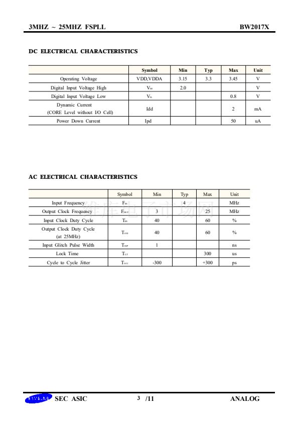
Fout : output clock frequency.
Fin :
reference input clock frequency.
M, P and S : values of programmable dividers.
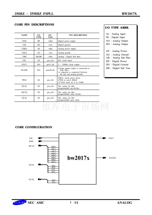
BW2017X consists of a phase and frequency detector(PFD),
a charge pump, an external loop filter, a voltage controlled
oscillator(VCO), a 4bit pre-divider P, an 8bit main divider M
and a 2bit post scaler S, and a lock detector as shown in
Figure1
IMPORTANT NOTICE
- Please contact SEC application engineer to confirm the proper selection of M,P,S value.
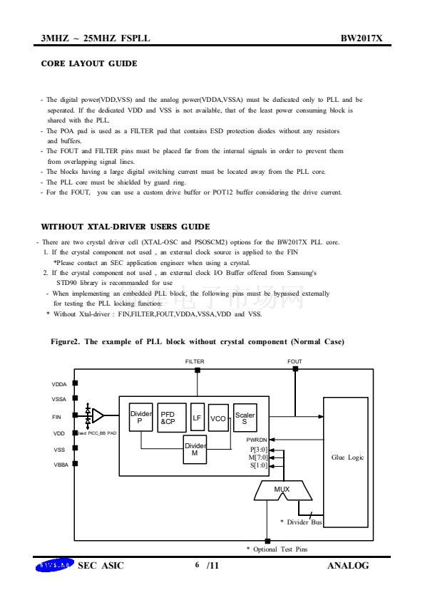
FUNCTIONAL BLOCK DIAGRAM
Fin
Pre
divider
P
PFD
charge
pump
Loop
Filter
(external)
VCO
Post
scaler
S
Fout
Filter
Main
divider
M
Figure 1. BW2017X Block Diagram
SAMSUNG ELECTRONICS Co. LTD


 1
1
 2
2
 3
3
 4
4
 5
5
 6
6
 7
7
 8
8
 9
9
 10
10
 11
11
 12
12
