20MHz ~ 100MHz FSPLL
General Description
The BW2011L is a Phase-Locked Loop (PLL)
frequency synthesizer constructed in CMOS on
single monolithic structure.
The PLL macrofunctions provide frequency
multiplication capabilities.
The output clock frequency FO is related
to the reference input clock frequency
Fin by the following equation:
FO = (ND*XIN ) /MD
Where,
Fout is the output clock frequency.
Fin is the reference input clock frequency.
m,p and s are the values for programmable dividers.
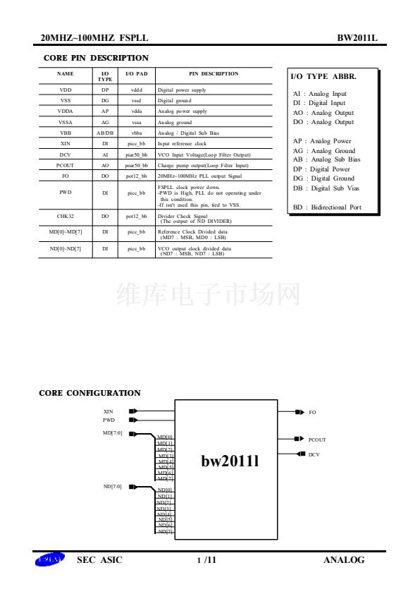
BW2011L consists of a phase/Frequency Detector(PFD),
a Charge Pump an External Loop Filter, a Voltage
Controlled Oscillator(VCO), a 8bit 2's complementary
counters as shown in Figure1.
BW2011L
DEC 1998 Version1.0
Features
鈼?/div>
0.35um CMOS device technology
鈼?/div>
3.3 Volt Single power supply
鈼?/div>
Output frequency range: 20~ 100 MHz
鈼?/div>
Jitter 鹵200ps
鈼?/div>
Duty ratio 40% to 60% at 100MHz
鈼?/div>
Frequency changed by programmable divider
鈼?/div>
Power down mode
IMPORTANT NOTICE
- Please contact SEC application engineer to confirm the proper selection of Divisor values.
FUNCTIONAL BLOCK DIAGRAM
Fref
XIN
REF Divider
MD
Fvco
PFD
Charge
Pump
Loop
Filter
(External)
VCO
FO
Main Divider
ND
Figure 1. Phase Lockd Loop Block Diagram
SAMSUNG ELECTRONICS Co. LTD
BW2011L相關型號PDF文件下載
-
型號
版本
描述
廠商
下載
-
英文版
BW2006L 100MHz~500MHz FSPLL BW2006L|Data Sheet
ETC
-
英文版
BW2010D 8Bit 250MSPS Triple DAC BW2010D|Data Sheet
ETC
-
英文版
BW2010P 25MHz ~ 250MHz FSPLL BW2010P|Data Sheet
ETC
-
英文版
BW2011L 20MHz ~ 100MHz FSPLL BW2011L|Data Sheet
ETC
-
英文版
BW2017X 3MHz ~ 25MHz FSPLL BW2017X|Data Sheet
ETC
-
英文版
BW2010AGP Frequency Doubler BW2010AGP|Data Sheet
ETC


 1
1
 2
2
 3
3
 4
4
 5
5
 6
6
 7
7
 8
8
 9
9
 10
10
 11
11
 12
12
