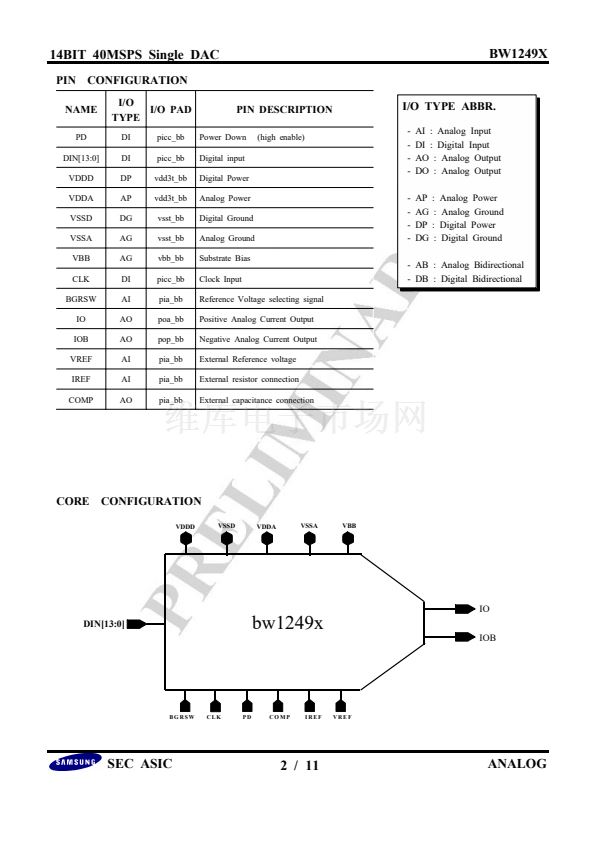
14BIT 40MSPS SINGLE DAC
BW1249X
GENERAL DESCRIPTION
This chip is a CMOS triple 14bit D/A
converter for general & video applications.
Its maximum conversion rate is 40MSPS
and supply voltage is 3.3V single. An
external(optional) or internal 1.24V reference
voltage(VREF) and a single external resister
control the full-scale output current.
It uses the two architecture of current-
segment and binerary-weighted.
FEATURES
*
*
*
*
*
*
*
*
*
*
*
*
40MSPS 1clock pipeline delay operation(Typ)
+3.3V CMOS monolithic construction
鹵
2.5LSB differential linearity (Typ)
鹵
5.0LSB integral linearity (Typ)
External or internal voltage reference
(Including Band Gap Reference Block)
Single Channel DAC
14-Bit parallel Digital input per channel
High impedance differential current output
Binary coding input
High impedance analog output current
source
Temperature : 0 ~ 70
擄
C
Power_Down
FUNCTIONAL BLOCK DIAGRAM
TYPICAL APPLICATION
8
_
IOB
*High Definition Television(DTV,HDD)
*High Resolution Color Graphics
*Hard Disk Driver
*CAE/CAD/CAM
*U_ADSL
*Image Processing
*Instrumentation
*Conventional Digital to Analog
Conversion
Second Latch
PD CNTRL
First Latch
14
SWITCH
Decoeder
DIN[13:0]
71
6
63
71
IO
COMP
CLK
CLKGEN
CM
OPA
BGR
BGRSW
VREF
PD
IREF
*
*
: Signal Flow
: Power_Down Control Flow
Ver 1.1 (Feb. 2000)
This datasheet is a preliminary version. No responsibility is
assumed by SEC for its use nor for any infringements of patents
or other rights of third parties that may result from its use. The
content of this datasheet is subject to change without any notice.
SAMSUNG ELECTRONICS Co. LTD
1 / 11


 1
1
 2
2
 3
3
 4
4
 5
5
 6
6
 7
7
 8
8
 9
9
 10
10
 11
11
