10BIT 500KSPS / 8BIT 650KSPS ADC
GENERAL DESCRIPTION
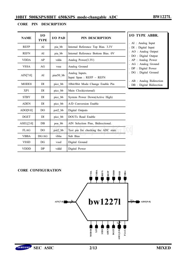
The BW1227L is a CMOS 8bit/10bit changeable A/D
converter which combines an 8-channel analog input
MUX, auto offset calibration comparator, high resolution
R-string DAC, clock generator, 8bit/10bit changeable
successive approximation register (SAR), output register,
and AISC
which controls analog input selection.
BW1227L provides a hardwired MODE8 pin and
software-selection power-down mode. At the MODE8
state is "low", the device operates as 10bit ADC, and if
"high", operates as 8bit. The device operates with a
single +3.3V supply and A/D conversion rate is
500KSPS at 10bit and 650KSPS at 8bit, external clock
XP1 is 25MHz. The operating temperature range is 0~70
擄C for commercial spec. Even if The BW1227L is
fabricated with 48TSSOP package but the USER can
select a fit package using the CORE.
BW1227L
FEATURES
-
-
-
-
-
Resolution : 10 bit
Differential Linearity Error : 鹵1.0 LSB
Integral Linearity Error : 鹵2.0 LSB
Maximum Conversion Rate : 500KSPS(10bit)
650KSPS(8bit)
Low Power Consumption
: at operating, 3.3mW(typ)
: at standby, 330nW(typ)
Power Supply Voltage : 3.3V single(typ)
Guaranteed Monotonicity
No Missing Code
Latched Tri-state Output
Operation Temperature Range : 0 ~70 擄C
-
-
-
-
-
FUNCTIONAL BLOCK DIAGRAM
VSSA
VDDA
REFN
REFP
VDDD
VSSD
VBBA
DAOUT
DAC
+
COP
SAR
10
MODE8
ADEN
FLAG
-
XP1
STBY
CKGEN
3
10
OUTREG
ADO[9:0]
DGET
AIN
AMUX
8
AISC
3
AIN[7:0]
ASEL[2:0]
Ver 1.5 (Apr. 2002)
No responsibility is assumed by SEC for its use nor for any infringements of patents
or other rights of third parties that may result from its use. The content of this data
sheet is subject to change without any notice.
SEC ASIC
ANALOG


 1
1
 2
2
 3
3
 4
4
 5
5
 6
6
 7
7
 8
8
 9
9
 10
10
 11
11
 12
12
 13
13
 14
14
 15
15
