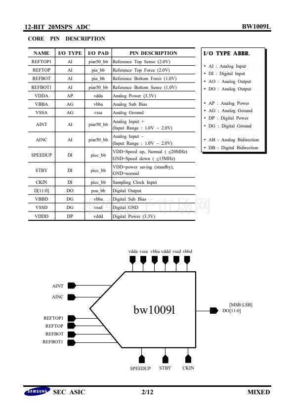
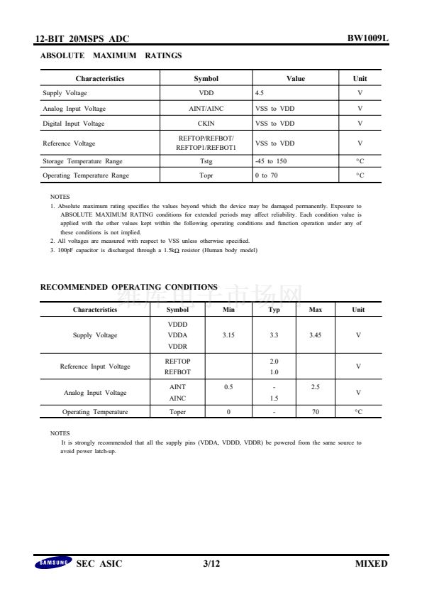
鈥?/div>
Resolution : 12-bit
Maximum Conversion Rate : 20MHz
Package Type : 48TSSOP
Power Supply : 3.3V
Power Consumption : 150mW (typical)
Reference Voltage : 2V, 1V (dual reference)
Input Range : 0.5V ~ 2.5V (2.0V
P-P
)
Differential Linearity Error : 鹵1.0 LSB
Integral Linearity Error : 鹵2.0 LSB
Signal to Noise & Distortion Ratio : 62dB
Digital Output : CMOS Level
Operating Temperature Range : 0擄C
~ 70
擄C
sampling rate of 20MHz.
The device is a monolithic ADC with an on-chip,
high-performance, sample-and-hold Amplifier (SHA)
and current reference.
The structure allows both
differential and single-ended input.
TYPICAL APPLICATIONS
High Definition TV (HDTV)
Video Applications
CCD Imaging (Copiers, Scanners, Cameras)
Medical Imaging
Digital Communications
FUNCTIONAL BLOCK DIAGRAM
Analog
Input
Reference
Input
SHA
MDAC
1
MDAC
2
MDAC
3
FLASH
1
FLASH
2
FLASH
3
FLASH
4
CML
GEN
MAIN
BIAS
Clock
CLOCK
GEN.
DIGITAL
LOGIC
Digital
Output
Ver 1.6 (Apr. 2002)
No responsibility is assumed by SEC for its use nor for any infringements of patents
or other rights of third parties that may result from its use. The content of this data
sheet is subject to change without any notice.
SAMSUNG ELECTRONICS Co. LTD


 1
1
 2
2
 3
3
 4
4
 5
5
 6
6
 7
7
 8
8
 9
9
 10
10
 11
11
 12
12
 13
13
