Philips Semiconductors
Product specification
TrenchMOS鈩?transistor
Standard level FET
GENERAL DESCRIPTION
N-channel enhancement mode
standard level field-effect power
transistor in a plastic envelope
suitable for surface mounting. Using
鈥檛rench鈥?technology, the device
features very low on-state resistance
and has integral zener diodes giving
ESD protection up to 2kV. It is
intended for use in automotive and
general
purpose
switching
applications.
BUK7830-30
QUICK REFERENCE DATA
SYMBOL
V
DS
I
D
P
tot
T
j
R
DS(ON)
PARAMETER
Drain-source voltage
Drain current (DC) T
sp
= 25 藲C
Drain current (DC) T
amb
= 25 藲C
Total power dissipation
Junction temperature
Drain-source on-state
resistance
V
GS
= 10 V
MAX.
30
12.8
5.9
8.3
150
30
UNIT
V
A
A
W
藲C
m鈩?/div>
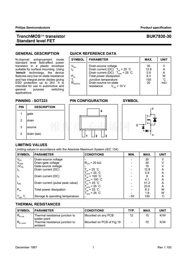
PINNING - SOT223
PIN
1
2
3
4
gate
drain
source
drain (tab)
DESCRIPTION
PIN CONFIGURATION
4
SYMBOL
d
g
s
1
2
3
LIMITING VALUES
Limiting values in accordance with the Absolute Maximum System (IEC 134)
SYMBOL
V
DS
V
DGR
鹵V
GS
I
D
I
D
I
DM
P
tot
T
stg
, T
j
PARAMETER
Drain-source voltage
Drain-gate voltage
Gate-source voltage
Drain current (DC)
Drain current (DC)
Drain current (pulse peak value)
Total power dissipation
Storage & operating temperature
CONDITIONS
-
R
GS
= 20 k鈩?/div>
-
T
sp
= 25 藲C
T
amb
= 25 藲C
T
sp
= 100 藲C
T
amb
= 100 藲C
T
sp
= 25 藲C
T
amb
= 25 藲C
T
sp
= 25 藲C
T
amb
= 25 藲C
-
MIN.
-
-
-
-
-
-
-
-
-
-
-
- 55
MAX.
30
30
16
12.8
5.9
9
4.1
51.2
23.6
8.3
1.8
150
UNIT
V
V
V
A
A
A
A
A
A
W
W
藲C
THERMAL RESISTANCES
SYMBOL
R
th j-sp
R
th j-amb
PARAMETER
Thermal resistance junction to
solder point
Thermal resistance junction to
ambient
CONDITIONS
Mounted on any PCB
Mounted on PCB of Fig.19
TYP.
12
-
MAX.
15
70
UNIT
K/W
K/W
December 1997
1
Rev 1.100


 1
1
 2
2
 3
3
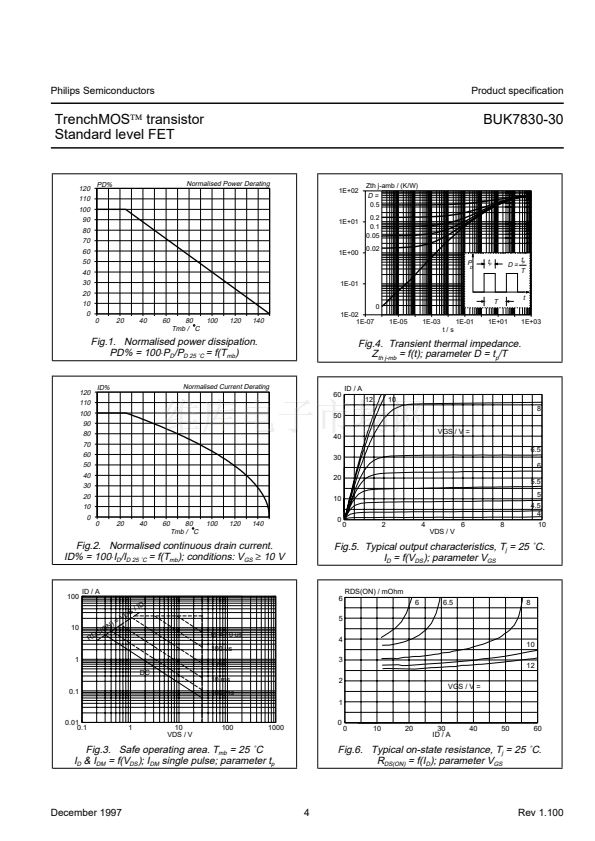 4
4
 5
5
 6
6
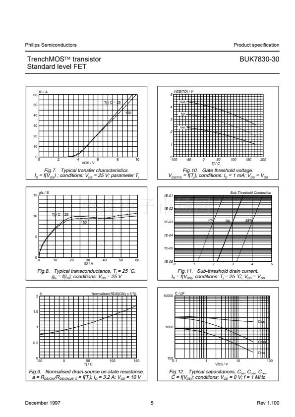
 7
7
 8
8
 9
9
 10
10
