Philips Semiconductors
Product specification
TrenchMOS餂?transistor
Standard level FET
GENERAL DESCRIPTION
N-channel enhancement mode
standard level field-effect power
transistor in a plastic envelope
suitable for surface mounting. Using
鈥檛rench鈥?technology the device
features
very
low
on-state
resistance. It is intended for use in
automotive and general purpose
switching applications.
BUK7640-100A
QUICK REFERENCE DATA
SYMBOL
V
DS
I
D
P
tot
T
j
R
DS(ON)
PARAMETER
Drain-source voltage
Drain current (DC)
Total power dissipation
Junction temperature
Drain-source on-state
resistance
V
GS
= 10 V
MAX.
100
37
138
175
40
UNIT
V
A
W
藲C
m鈩?/div>
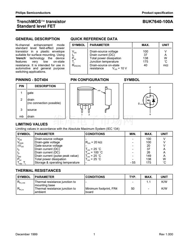
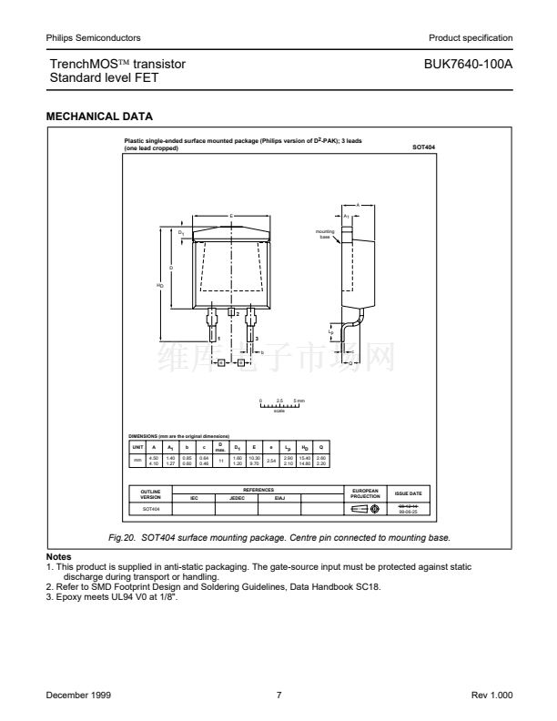
PINNING - SOT404
PIN
1
2
3
mb
gate
drain
(no connection possible)
source
drain
DESCRIPTION
PIN CONFIGURATION
mb
SYMBOL
d
g
2
1
3
s
LIMITING VALUES
Limiting values in accordance with the Absolute Maximum System (IEC 134)
SYMBOL
V
DS
V
DGR
鹵V
GS
I
D
I
D
I
DM
P
tot
T
stg
, T
j
PARAMETER
Drain-source voltage
Drain-gate voltage
Gate-source voltage
Drain current (DC)
Drain current (DC)
Drain current (pulse peak value)
Total power dissipation
Storage & operating temperature
CONDITIONS
-
R
GS
= 20 k鈩?/div>
-
T
mb
= 25 藲C
T
mb
= 100 藲C
T
mb
= 25 藲C
T
mb
= 25 藲C
-
MIN.
-
-
-
-
-
-
-
- 55
MAX.
100
100
20
37
26
149
138
175
UNIT
V
V
V
A
A
A
W
藲C
THERMAL RESISTANCES
SYMBOL
R
th j-mb
R
th j-a
PARAMETER
Thermal resistance junction to
mounting base
Thermal resistance junction to
ambient
CONDITIONS
-
Minimum footprint, FR4
board
TYP.
-
50
MAX.
1.1
-
UNIT
K/W
K/W
December 1999
1
Rev 1.000


 1
1
 2
2
 3
3
 4
4
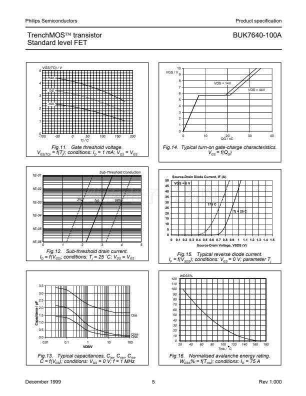 5
5
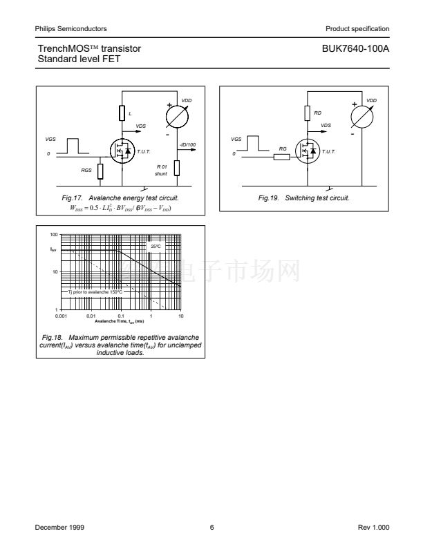 6
6
 7
7
 8
8
