Philips Semiconductors
Product specification
Silicon Diffused Power Transistor
BUJ100AT
GENERAL DESCRIPTION
High-voltage, high-speed planar-passivated npn power switching transistor in the SOT223 envelope intended for
use in compact fluorescent lamps, low power electronic lighting ballasts and similar high frequency converters and
inverters.
QUICK REFERENCE DATA
SYMBOL
V
CESM
V
CBO
V
CEO
I
C
I
CM
P
tot
V
CEsat
h
FE
t
fi
PARAMETER
Collector-emitter voltage peak value
Collector-Base voltage (open emitter)
Collector-emitter voltage (open base)
Collector current (DC)
Collector current peak value
Total power dissipation
Collector-emitter saturation voltage
Fall time (Inductive)
CONDITIONS
V
BE
= 0 V
TYP.
-
-
-
-
-
-
0.23
14
50
MAX.
700
700
400
1.0
2.0
6
1.0
20
70
UNIT
V
V
V
A
A
W
V
ns
T
sp
鈮?/div>
25 藲C
I
C
= 0.75 A;I
B
= 150 mA
I
C
= 0.75 A;V
CE
= 5 V
I
C
= 1.0 A,I
BON
=200 mA
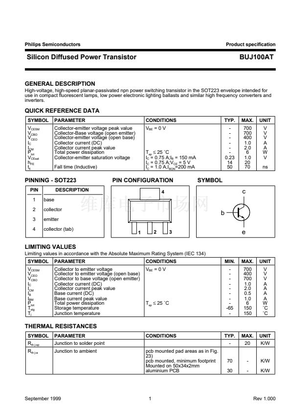
PINNING - SOT223
PIN
1
2
3
4
base
collector
emitter
collector (tab)
DESCRIPTION
PIN CONFIGURATION
4
SYMBOL
c
b
1
2
3
e
LIMITING VALUES
Limiting values in accordance with the Absolute Maximum Rating System (IEC 134)
SYMBOL
V
CESM
V
CEO
V
CBO
I
C
I
CM
I
B
I
BM
P
tot
T
stg
T
j
PARAMETER
Collector to emitter voltage
Collector to emitter voltage (open base)
Collector to base voltage (open emitter)
Collector current (DC)
Collector current peak value
Base current (DC)
Base current peak value
Total power dissipation
Storage temperature
Junction temperature
CONDITIONS
V
BE
= 0 V
MIN.
-
-
-
-
-
-
-
-
-65
-
MAX.
700
400
700
1.0
2.0
0.5
1.0
6
150
150
UNIT
V
V
V
A
A
A
A
W
藲C
藲C
T
sp
鈮?/div>
25 藲C
THERMAL RESISTANCES
SYMBOL
R
th j-sp
R
th j-a
PARAMETER
Junction to solder point
Junction to ambient
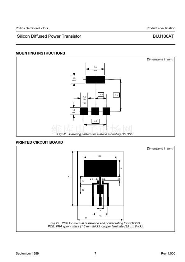
pcb mounted pad areas as in Fig.
23)
pcb mounted, minimum footprint
Mounted on 50x34x2mm
aluminium PCB
CONDITIONS
TYP.
-
MAX.
20
UNIT
K/W
70
30
-
-
K/W
K/W
September 1999
1
Rev 1.000


 1
1
 2
2
 3
3
 4
4
 5
5
 6
6
 7
7
 8
8
 9
9
