BLV7002
BLV7002 N-channel Enhancement Mode
Vertical D-MOS Transistor Chip
Description
N-channel enhancement mode field-effect transistor
Features
Very fast switching
Logic level compatible
Applications
Relay driver
High speed line driver
Logic level translator.
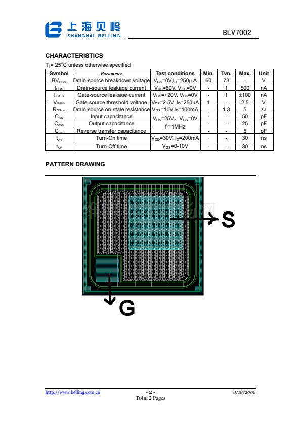
Size
Chip size: 495碌m 脳490碌m
structure
Planar type
Electrodes: Aluminum alloy
Backside metal: Au alloy
Scribe street width: 50碌m
Pad size: 90碌m x90碌m
Die per wafer: 25800
ABSOLUTE MAXIMUM RATING
Symbol
V
DS
V
GS
I
D
I
DM
P
tot
T
STG
T
j
Parameter
Drain 鈥?source voltage (DC)
Gate 鈥?source voltage (DC)
Drain current (DC)
Peak drain current
Total power dissipation
Storage temperature
Junction temperature
Min.
-
-
-
-
-
-55
-
Max.
60
鹵20
115
0.46
0.2
+150
150
Unit
V
V
mA
A
W
o
C
o
C
http://www.belling.com.cn
-1-
Total
2 Pages
8/18/2006


 1
1
 2
2
