B5S162862
20-BIT TWO PORT BUS SWITCH WITH FOUR ENABLE
CONTROL AND 25鈩?SERIES RESISTOR IN OUTPUT
PRELIMINARY DATA
s
s
s
s
s
s
s
s
s
HIGH SPEED: t
PD
= 1.25ns (MAX.)
at V
CC
= 4.5V T
A
=85擄C
ON RESISTANCE BETWEEN TWO PORT:
25鈩?(TYP) at V
CC
= 5.0V T
A
=25擄C
LOW POWER DISSIPATION:
I
CC
= 1uA(MAX.) at T
A
=25擄C
COMPATIBLE WITH TTL OUTPUTS:
V
IH
=2V(MIN), V
IL
=0.8V(MAX)
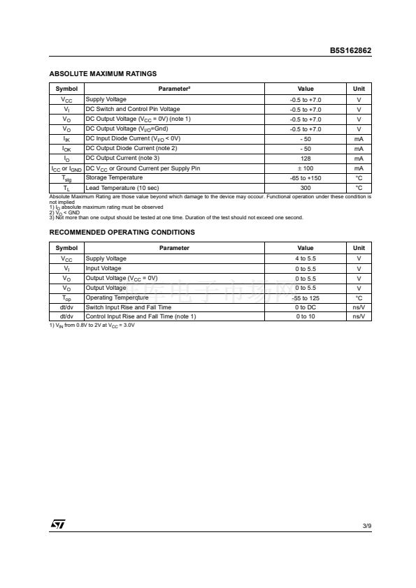
POWER DOWN PROTECTION ON INPUTS
AND OUTPUTS
OPERATING VOLTAGE RANGE:
V
CC
(OPR) = 4V to 5.5V
PIN AND FUNCTION COMPATIBLE WITH
74 SERIES 16862
IMPROVED LATCH-UP IMMUNITY
ESD PERFORMANCE:
HBM > 2000V (MIL STD 883 method 3015);
MM > 200V
TSSOP
ORDER CODES
PACKAGE
TSSOP48
T&R
B5S162861TTR
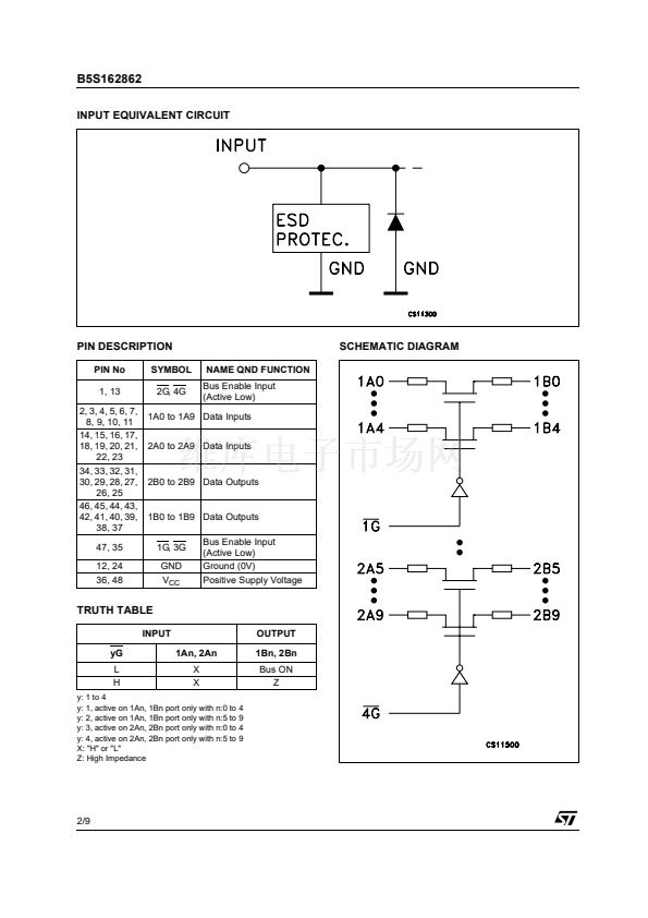
PIN CONNECTION
DESCRIPTION
The B5S162862 is an advanced high-speed
CMOS 20-BIT TWO PORT BUS SWITCH
fabricated with sub-micron silicon gate and
double-layer metal wiring C
2
MOS tecnology.
It is ideal for 4V to 5.5V V
CC
operations and
ultra-low power and low noise applications,
typically notebook and docking station.
Any nG output control governs four 5-bit BUS
SWITCHES. Output Enable inputs (nG) tied
together gives full 20-bit operations. When nG is
LOW, the switches are on. When nG is HIGH, the
switches are in high impedance state.
It has ultra high-speed performance at 5V near
zero delay with low ON resistance and include
25鈩?series resistor to reduce noise resulting from
reflections, thus eliminating the need for an
external terminating resistor.
All inputs and outputs are equipped with
protection circuits against static discharge, giving
them 2KV ESD immunity and transient excess
voltage.
February 2003
1/9
This is preliminary information on a new product now in development are or undergoing evaluation. Details subject to change without notice.


 1
1
 2
2
 3
3
 4
4
 5
5
 6
6
 7
7
 8
8
 9
9
