鈥?/div>
3.0V to 5.5V Operating Range
Advanced Low Voltage, Zero Power,
Electrically Erasable Programmable Logic Device
Edge-Sensing 鈥淶ero鈥?Power
Low Voltage Equivalent of ATF22V10CZ
鈥淶ero鈥?Standby Power (25
碌A
Maximum)
Ideal for Battery Powered Systems
25 ns Maximum Propagation Delay
CMOS and TTL Compatible Inputs and Outputs
Latch Feature Hold Inputs to Previous Logic States
Advanced E
2
Technology
Reprogrammable
100% Tested
High Reliability CMOS Process
20 Year Data Retention
100 Erase/Write Cycles
2,000V ESD Protection
200 mA Latchup Immunity
Commercial and Industrial Temperature Ranges
Dual-in-Line and Surface Mount Standard Pinouts
High
Performance
E
2
PLD
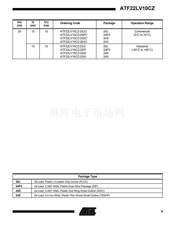
ATF22LV10CZ
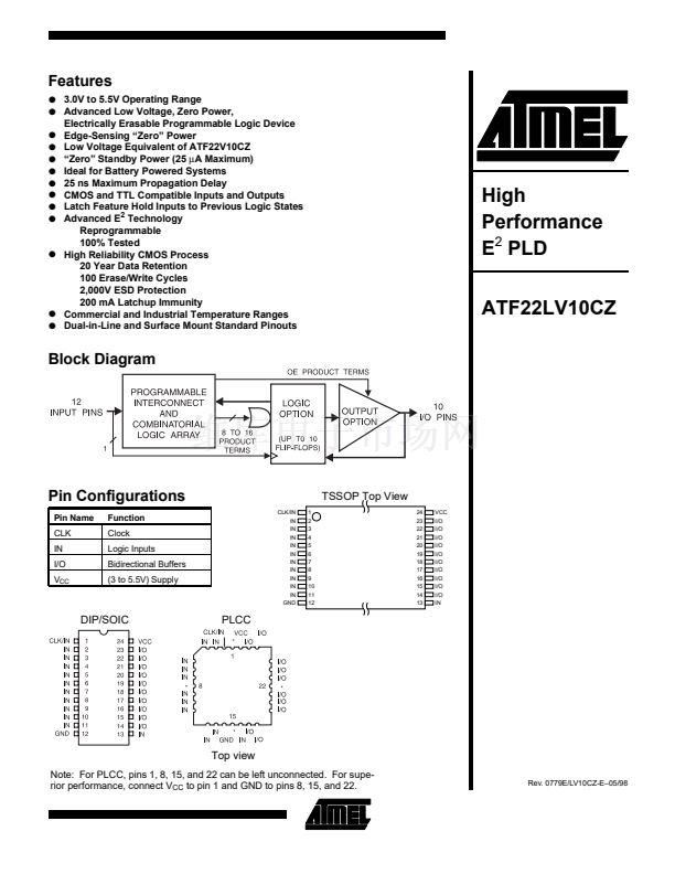
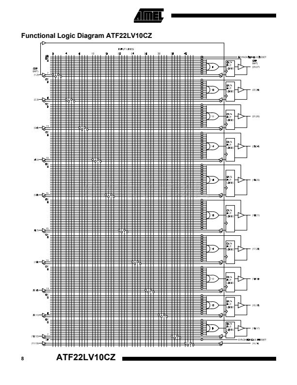
Block Diagram
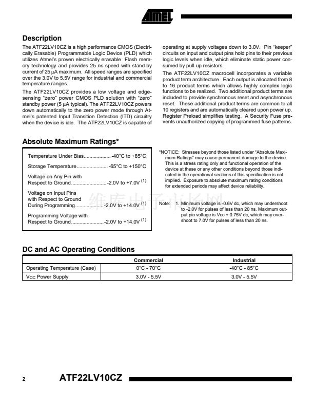
Pin Configurations
Pin Name
CLK
IN
I/O
V
CC
Function
Clock
Logic Inputs
Bidirectional Buffers
(3 to 5.5V) Supply
CLK/IN
IN
IN
IN
IN
IN
IN
IN
IN
IN
IN
GND
1
2
3
4
5
6
7
8
9
10
11
12
TSSOP Top View
24
23
22
21
20
19
18
17
16
15
14
13
VCC
I/O
I/O
I/O
I/O
I/O
I/O
I/O
I/O
I/O
I/O
IN
ATF22LV10CZ
DIP/SOIC
PLCC
Top view
Note: For PLCC, pins 1, 8, 15, and 22 can be left unconnected. For supe-
rior performance, connect V
CC
to pin 1 and GND to pins 8, 15, and 22.
Rev. 0779E/LV10CZ-E鈥?5/98


 1
1
 2
2
 3
3
 4
4
 5
5
 6
6
 7
7
 8
8
 9
9
