鈥?/div>
Operating Conditions
IO25 and IO33 Pad Libraries Provide Interfaces to 2.5V and 3V Environments
Oscillators Provide Stable Clock Sources
Basic Analog Input/Output, Power, Ground and Multiplexer Cells Available,
High-performance Analog Cells Can Be Developed on Request
Memory Cells Compiled to the Precise Requirements of the Design
Compatible with Atmel鈥檚 Extensive Range of Microcontroller, DSP, Standard-interface
and Application-specific Cells
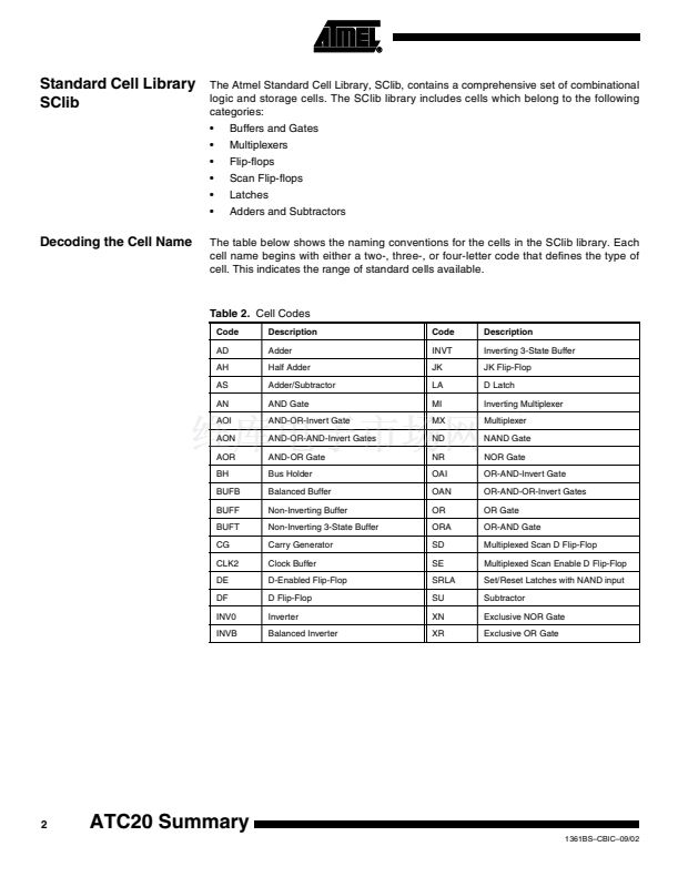
Cell-based ASIC
ATC20
Summary
Description
The Atmel ATC20 CBIC family is fabricated on a proprietary 0.21 micron five-layer-
metal CMOS process intended for use with a supply voltage of 1.8V 鹵 0.15V. The fol-
lowing table shows the range for which Atmel library cells have been characterized.
Table 1.
Recommended Operating Conditions
Symbol
V
DD
V
DD2.5
V
DD3.3
V
I
V
O
TEMP
Parameter
DC Supply Voltage
DC Supply Voltage
DC Supply Voltage
DC Input Voltage
DC Output Voltage
Operating Free Air
Temperature Range
Industrial
Conditions
Core and Standard I/Os
2.5V Interface I/Os
3V Interface I/Os
Min
1.65
2.25
3
0
0
-40
Typ
1.8
2.5
3.3
Max
1.95
2.75
3.6
V
DD
V
DD
+85
Unit
V
V
V
V
V
擄
C
The Atmel cell libraries and megacell compilers have been designed in order to be
compatible with each other. Simulation representations exist for three types of operat-
ing conditions. They correspond to three characterization conditions defined as
follows:
鈥?/div>
MIN conditions:
鈥?/div>
鈥?/div>
鈥?/div>
鈥?/div>
鈥?/div>
鈥?/div>
鈥?/div>
鈥?/div>
鈥?/div>
鈥?/div>
鈥?/div>
T
J
= -40擄C
V
DD
(cell) = 1.95V
Process = fast (industrial best case)
T
J
= +25擄C
V
DD
(cell) = 1.8V
Process = typ (industrial typical case)
T
J
= +100擄C
V
DD
(cell) = 1.65V
Process = slow (industrial worst case)
TYP conditions:
MAX conditions:
Delays to tri-state are defined as delay to turn off (VGS < VT) of the driving devices.
Output pad drain current corresponds to the output current of the pad when the output
voltage is V
OL
or V
OH
. The output resistor of the pad and the voltage drop due to
access resistors (in and out of the die) are taken into account. In order to have accu-
rate timing estimates, all characterization has been run on electrical netlists extracted
from the layout database.
Rev. 1361BS鈥揅BIC鈥?9/02
1
ATC20相關(guān)型號(hào)PDF文件下載
-
型號(hào)
版本
描述
廠商
下載
-
英文版
ATC20 Summary [Updated 9/02. 11 Pages] The ATC20 Cell-based ...
ETC
-
英文版
ATC20 Summary [Updated 9/02. 11 Pages] The ATC20 Cell-based ...
-
英文版
Cell-based ASIC
-
英文版
Cell-based ASIC
ATMEL [ATM...
-
英文版
SWITCH BOX 2 WAY+LEAD
ETC
-
英文版
CAMERA PIR +INFRA RED
ETC
-
英文版
Integrated Power Conversion and Power Management Solution
ARTESYN
-
英文版
Dual-Input Bus Converter
-
英文版
Dual-Input Bus Converter
EMERSON-NETWORK...
-
英文版
Dual-Input Bus Converter
ATMEL [ATM...
-
英文版
The ATC20 CBIC family is fabricated on a proprietary 0.21 mi...
-
英文版
The ATC25 CBIC family is designed to operate with a supply v...
-
英文版
Dual-Input Bus Converter
-
英文版
Integrated Power Conversion and Power Management Solution
ARTESYN
-
英文版
Dual-Input Bus Converter
EMERSON-NETWORK...
-
英文版
Dual-Input Bus Converter
ATMEL [ATM...


 1
1
 2
2
 3
3
 4
4
 5
5
 6
6
 7
7
 8
8
 9
9
 10
10
 11
11
