鈥?/div>
Dual-in-line and Surface Mount Packages
Low-voltage UV
Erasable
Programmable
Logic Device
AT22LV10
AT22LV10L
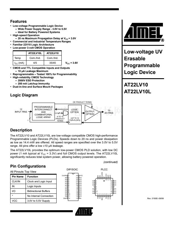
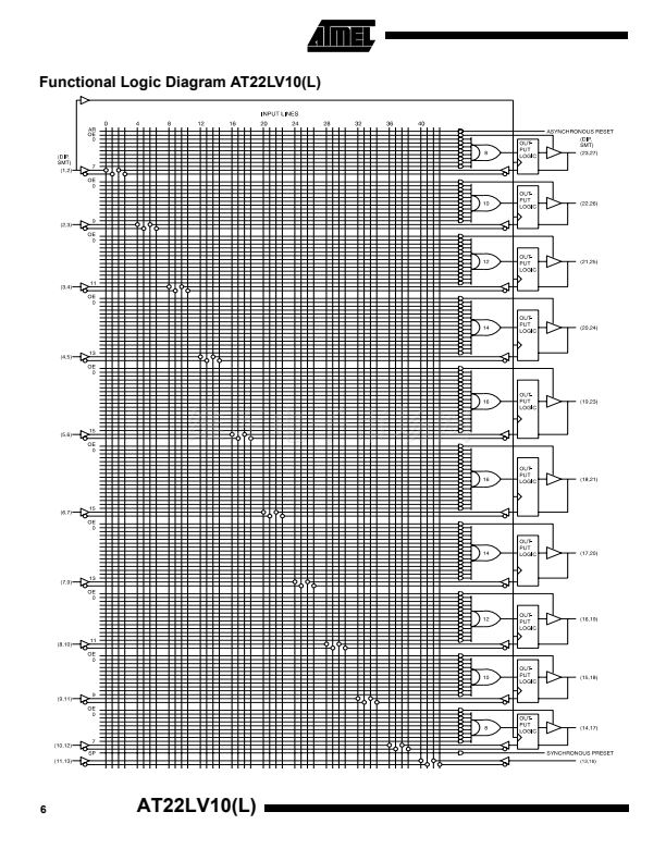
Logic Diagram
Description
The AT22LV10 and AT22LV10L are low-voltage compatible CMOS high-performance
Programmable Logic Devices (PLDs). Speeds down to 20 ns and power dissipation
as low as 14.4 mW are offered. All speed ranges are specified over the 3.0V to 5.5V
range. All pins offer a low
鹵
10 碌A(chǔ) leakage.
The AT22LV10L provides the optimum low-power CMOS PLD solution, with low DC
power (1 mA typical at V
CC
= 3.3V) and full CMOS output levels. The AT22LV10L
significantly reduces total system power, allowing battery powered operation.
(continued)
Pin Configurations
Pin Name
CLK/IN
IN
I/O
*
VCC
Function
Clock and Logic Input
Logic Inputs
Bidirectional Buffers
No Internal Connection
3.0V to 5.5V Supply
CLK/IN
IN
IN
IN
IN
IN
IN
IN
IN
IN
IN
GND
1
2
3
4
5
6
7
8
9
10
11
12
24
23
22
21
20
19
18
17
16
15
14
13
VCC
I/O
I/O
I/O
I/O
I/O
I/O
I/O
I/O
I/O
I/O
IN
IN
IN
CLK/IN
*
VCC
I/O
I/O
4
3
2
1
28
27
26
IN
IN
GND
*
IN
I/O
I/O
12
13
14
15
16
17
18
IN
IN
IN
*
IN
IN
IN
5
6
7
8
9
10
11
25
24
23
22
21
20
19
I/O
I/O
I/O
*
I/O
I/O
I/O
All Pinouts Top View
DIP/SOIC
PLCC
Rev. 0190E鈥?8/99
1


 1
1
 2
2
 3
3
 4
4
 5
5
 6
6
 7
7
 8
8
 9
9
 10
10
 11
11
 12
12
