July 2005
rev 0.4
2.5V and 3.3V LVCMOS Clock Distribution Buffer
Features
Configurable
10
outputs
LVCMOS
clock
distribution buffer
Compatible to single, dual and mixed 3.3V/2.5V
Voltage supply
Wide range output clock frequency up to 250MHz
Designed for mid-range to high-performance
telecom, networking and computer applications
Supports applications requiring clock redundancy
Max. output skew of 200pS (150pS within one
bank)
Selectable output configurations per output bank
Tristatable outputs
32 lead LQFP & TQFP Packages
Ambient operating temperature range of
-40 to 85擄C
-
ASM2I99446
is specified for the extended temperature range of -40擄C to
85擄C.
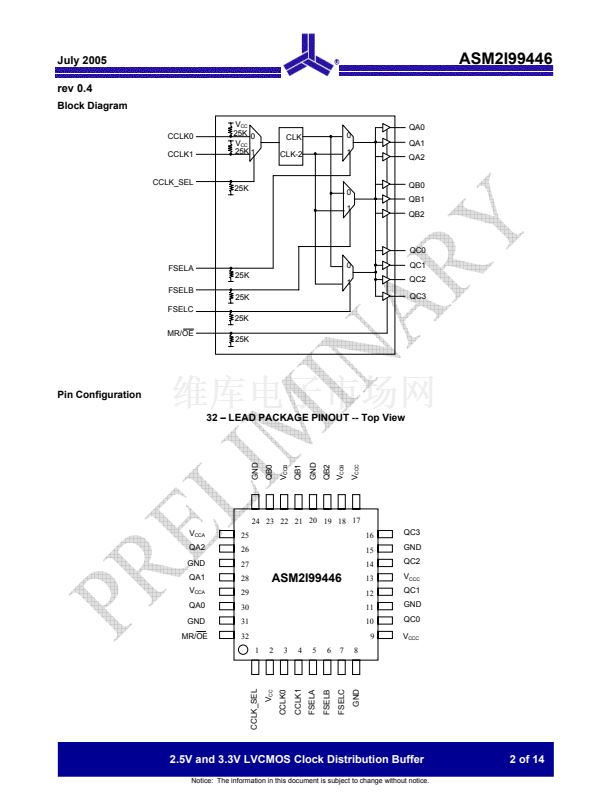
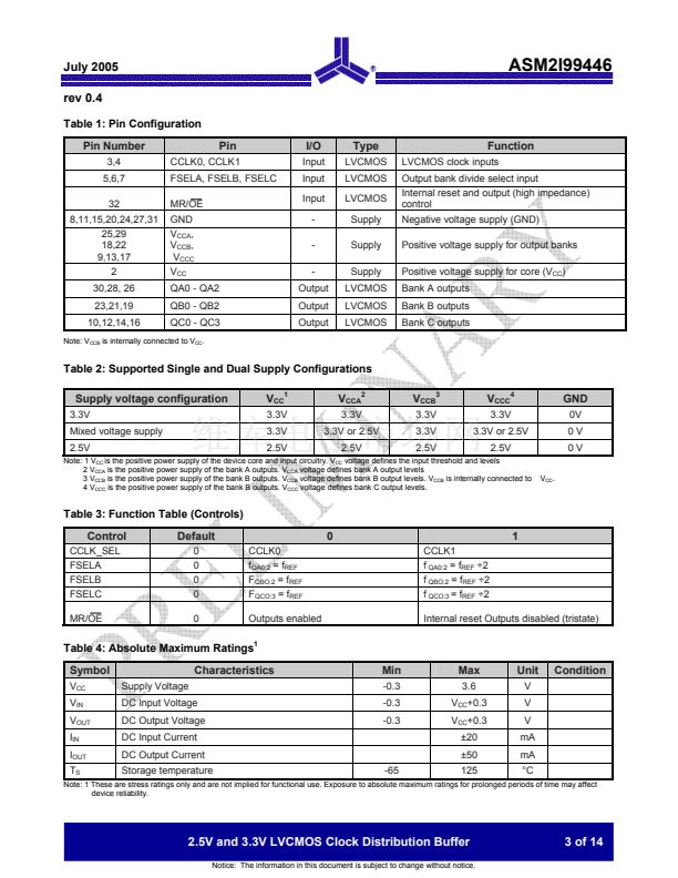
The ASM2I99446 is a full static fanout buffer design
supporting clock frequencies up to 250MHz. The signals
are generated and retimed on-chip to ensure minimal skew
between the three output banks. Two independent
LVCMOS compatible clock inputs are available. This
feature supports redundant clock sources or the addition of
a test clock into the system design. Each of the three
output banks can be individually supplied by 2.5V or 3.3V
supporting mixed voltage applications. The FSELx pins
choose between division of the input reference frequency
by one or two. The frequency divider can be set individually
for each of the three output banks. The ASM2I99446 can
be reset and the outputs are disabled by deasserting the
MR/OE pin (logic high state). Asserting MR/OE will enable
the outputs.
Functional Description
The ASM2I99446 is a 2.5V and 3.3V compatible 1:10 clock
distribution buffer designed for low-voltage mid-range to
high-performance telecom, networking and computing
applications. Both 3.3V, 2.5V and dual supply voltages are
supported for mixed-voltage applications. The ASM2I99446
offers 10 low-skew outputs and 2 selectable inputs for clock
redundancy. The outputs are configurable and support 1:1
and 1:2 output to input frequency ratios. The ASM2I99446
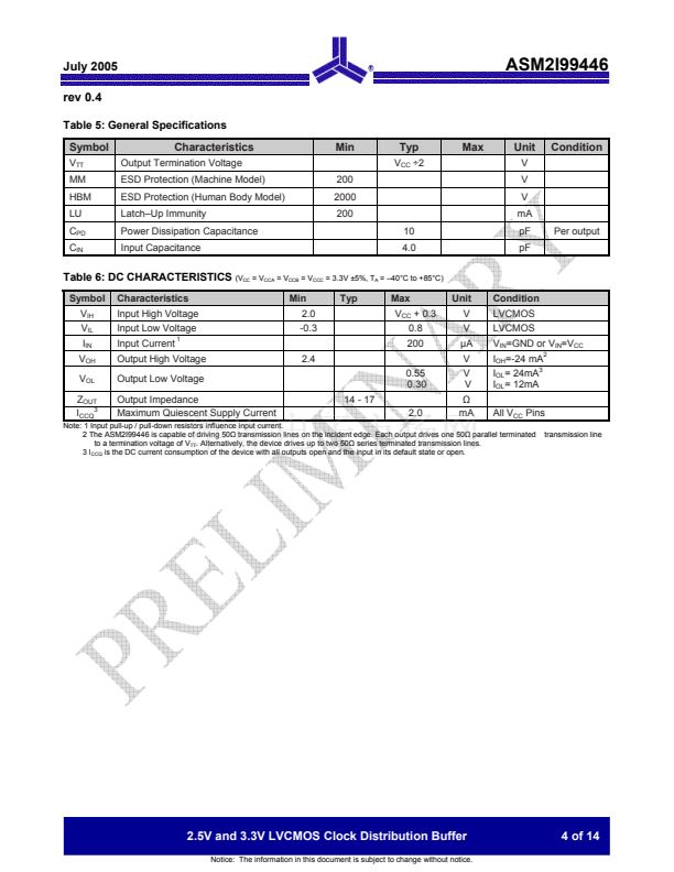
All inputs accept LVCMOS signals while the outputs
provide LVCMOS compatible levels with the capability to
drive terminated 50
鈩?/div>
transmission lines. Please consult the
ASM2I99456 specification for a 1:10 mixed voltage buffer
with LVPECL compatible inputs. For series terminated
transmission lines, each of the ASM2I99446 outputs can
drive one or two traces giving the devices an effective
fanout of 1:20. The device is packaged in a
32-lead LQFP and TQFP Packages.
7x7mm
2
Alliance Semiconductor
2575, Augustine Drive
鈥?/div>
Santa Clara, CA
鈥?/div>
Tel: 408.855.4900
鈥?/div>
Fax: 408.855.4999
鈥?/div>
www.alsc.com
Notice: The information in this document is subject to change without notice.
ASM2I99446-32-ET相關(guān)型號(hào)PDF文件下載
-
型號(hào)
版本
描述
廠商
下載
-
英文版
VERY LOW-COST VOICE SYNTHESIZER WITH 4-BIT MICROPROCESSOR
APLUS
-
英文版
-
英文版
VERY LOW-COST VOICE SYNTHESIZER WITH 4-BIT MICROPROCESSOR
APLUS
-
英文版
VERY LOW-COST VOICE SYNTHESIZER WITH 4-BIT MICROPROCESSOR
APLUS [Apu...
-
英文版
VERY LOW-COST VOICE SYNTHESIZER WITH 4-BIT MICROPROCESSOR
APLUS
-
英文版
VERY LOW-COST VOICE SYNTHESIZER WITH 4-BIT MICROPROCESSOR
APLUS [Apu...
-
英文版
VERY LOW-COST VOICE SYNTHESIZER WITH 4-BIT MICROPROCESSOR
APLUS
-
英文版
VERY LOW-COST VOICE SYNTHESIZER WITH 4-BIT MICROPROCESSOR
APLUS [Apu...
-
英文版
VERY LOW-COST VOICE SYNTHESIZER WITH 4-BIT MICROPROCESSOR
APLUS
-
英文版
VERY LOW-COST VOICE SYNTHESIZER WITH 4-BIT MICROPROCESSOR
APLUS [Apu...
-
英文版
Low Voltage 1:18 Clock Distribution Chip
ALSC
-
英文版
Low Voltage 1:18 Clock Distribution Chip
ALSC [Alli...
-
英文版
Low Voltage 1:18 Clock Distribution Chip
ALSC
-
英文版
Low Voltage 1:18 Clock Distribution Chip
ALSC [Alli...
-
英文版
Low Voltage 1:18 Clock Distribution Chip
ALSC
-
英文版
Low Voltage 1:18 Clock Distribution Chip
ALSC [Alli...
-
英文版
2.5V and 3.3V LVCMOS Clock Distribution Buffer
ALSC
-
英文版
2.5V and 3.3V LVCMOS Clock Distribution Buffer
ALSC [Alli...
-
英文版
3.3V/2.5V 1:9 LVCMOS Clock Fanout Buffer
ALSC
-
英文版
3.3V/2.5V 1:9 LVCMOS Clock Fanout Buffer
ALSC [Alli...


 1
1
 2
2
 3
3
 4
4
 5
5
 6
6
 7
7
 8
8
 9
9
 10
10
 11
11
 12
12
 13
13
 14
14
