May 2001
廬
AS7C256
AS7C3256
5V/3.3V 32K X 8 CMOS SRAM (Common I/O)
Features
鈥?AS7C256 (5V version)
鈥?AS7C3256 (3.3V version)
鈥?Industrial and commercial temperature
鈥?Organization: 32,768 words 脳 8 bits
鈥?High speed
- 12/15/20 ns address access time
- 6, 7, 8 ns output enable access time
鈥?Very low power consumption: STANDBY
- 22 mW (AS7C256) / max CMOS I/O
- 7.2 mW (AS7C3256) / max CMOS I/O
鈥?Easy memory expansion with CE and OE inputs
鈥?TTL-compatible, three-state I/O
鈥?28-pin JEDEC standard packages
- 300 mil PDIP
- 300 mil SOJ
- 8
脳
13.4 mm TSOP 1
鈥?Very low power consumption: ACTIVE
- 660mW (AS7C256) / max @ 12 ns
- 216mW (AS7C3256) / max @ 12 ns
鈥?ESD protection
鈮?/div>
2000 volts
鈥?Latch-up current
鈮?/div>
200 mA
Logic block diagram
V
CC
GND
Input buffer
Pin arrangement
28-pin TSOP 1 (8脳13.4 mm)
28-pin DIP, SOJ (300 mil)
A0
A1
A2
A3
A4
A5
A6
A14
I/O7
Row decoder
Sense amp
256 X 128 X 8
Array
(262,144)
I/O0
OE
A11
A9
A8
A13
WE
V
CC
A14
A12
A7
A6
A5
A4
A3
1
2
3
4
5
6
7
8
9
10
11
12
13
14
(22)
(23)
(24)
(25)
(26)
(27)
(28) AS7C256
(1) AS7C3256
(2)
(3)
(4)
(5)
(6)
(7)
(21) 28
(20) 27
(19) 26
(18) 25
(17) 24
(16) 23
(15) 22
(14) 21
(13) 20
(12) 19
(11) 18
(10) 17
(9) 16
(8) 15
A10
CE
I/O7
I/O6
I/O5
I/O4
I/O3
GND
I/O2
I/O1
I/O0
A0
A1
A2
Note: This part is compatible with both pin numbering
conventions used by various manufacturers.
Column decoder
WE
Control
circuit
A
7
A
8
A A A A A
9 10 11 12 13
OE
CE
A14
A12
A7
A6
A5
A4
A3
A2
A1
A0
I/O0
I/O1
I/O2
GND
1
2
3
4
5
6
7
8
9
10
11
12
13
14
28
27
26
25
24
23
22
21
20
19
18
17
16
15
V
CC
WE
A13
A8
A9
A11
OE
A10
CE
I/O7
I/O6
I/O5
I/O4
I/O3
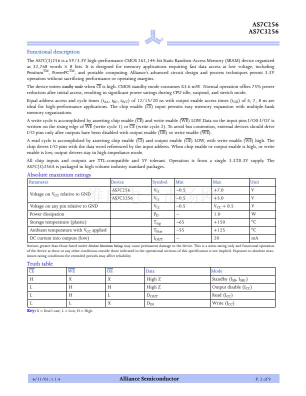
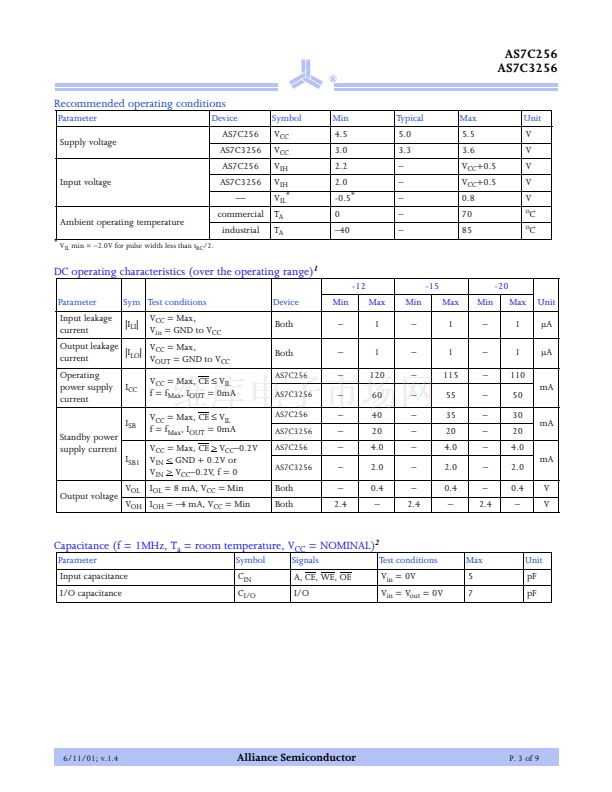
Selection guide
AS7C256-12
AS7C3256-12
AS7C256-15
AS7C3256-15
AS7C256-20
AS7C3256-20
Unit
Maximum address access time
Maximum output enable access time
Maximum operating current
Maximum CMOS standby current
AS7C256
AS7C3256
AS7C256
AS7C3256
12
6
120
60
4
2
15
7
115
55
4
2
20
8
110
50
4
2
AS7C256
AS7C3256
ns
ns
mA
mA
mA
mA
6/11/01; v.1.4
Alliance Semiconductor
P. 1 of 9
Copyright 漏 Alliance Semiconductor. All rights reserved.


 1
1
 2
2
 3
3
 4
4
 5
5
 6
6
 7
7
 8
8
 9
9
