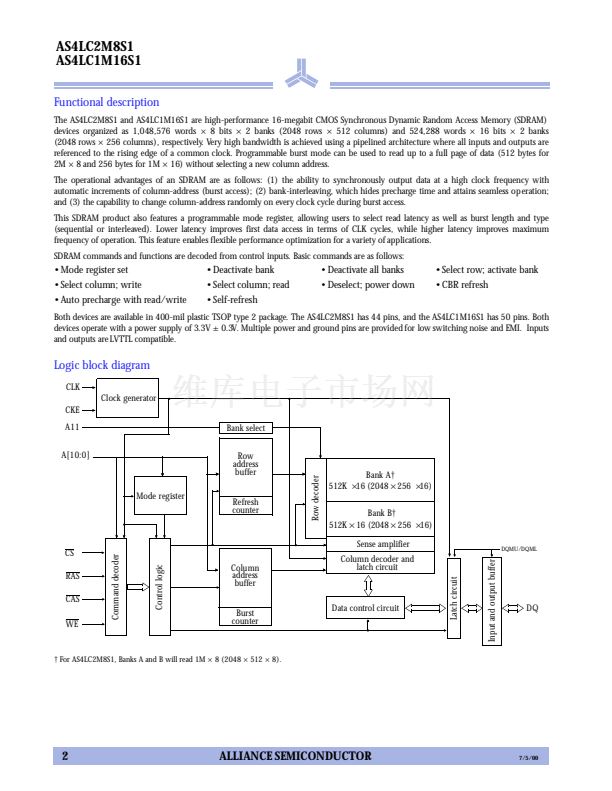
Advance information
3.3V 2M
脳
8/1M
脳
16 CMOS synchronous DRAM
Features
鈥?Organization
- 1,048,576 words 脳 8 bits 脳 2 banks (2M 脳 8)
11 row, 9 column address
- 524,288 words 脳 16 bits 脳 2 banks (1M 脳 16)
11 row,8 column address
AS4LC2M8S1
AS4LC1M16S1
鈥?All signals referenced to positive edge of clock, fully
synchronous
鈥?Dual internal banks controlled by A11 (bank select)
鈥?High speed
- 143/125/100 MHz
- 7/8/10 ns clock access time
鈥?PC100 functionality
鈥?Automatic and direct precharge including concurrent
autoprecharge
鈥?Burst read, write/Single write
鈥?Random column address assertion in every cycle, pipelined
operation
鈥?LVTTL compatible I/O
鈥?3.3V power supply
鈥?JEDEC standard package, pinout and function
- 400 mil, 44-pin TSOP II (2M 脳 8)
- 400 mil, 50-pin TSOP II (1M 脳 16)
鈥?Low power consumption
- Active: 576 mW max
- Standby: 7.2 mW max, CMOS I/O
鈥?2048 refresh cycles, 64 ms refresh interval
鈥?Auto refresh and self refresh (2K self refresh mode at 64 ms)
鈥?Read/write data masking
鈥?Programmable burst length (1/2/4/8/ full page)
鈥?Programmable burst sequence (sequential/interleaved)
鈥?Programmable CAS latency (1/2/3)
Pin arrangement
TSOP II
V
CC
DQ0
V
SSQ
DQ1
V
CCQ
DQ2
V
SSQ
DQ3
V
CCQ
NC
NC
WE
CAS
RAS
CS
A11
A10
A0
A1
A2
A3
V
CC
1
2
3
4
5
6
7
8
9
10
11
12
13
14
15
16
17
18
19
20
21
22
44
43
42
41
40
39
38
37
36
35
34
33
32
31
30
29
28
27
26
25
24
23
V
SS
DQ7
V
SSQ
DQ6
V
CCQ
DQ5
V
SSQ
DQ4
V
CCQ
NC
NC
DQM
CLK
CKE
NC
A9
A8
A7
A6
A5
A4
V
SS
V
CC
DQ0
DQ1
V
SSQ
DQ2
DQ3
V
CCQ
DQ4
DQ5
V
SSQ
DQ6
DQ7
V
CCQ
LDQM
WE
CAS
RAS
CS
A11
A10
A0
A1
A2
A3
V
CC
1
2
3
4
5
6
7
8
9
10
11
12
13
14
15
16
17
18
19
20
21
22
23
24
25
TSOP II
50
49
48
47
46
45
44
43
42
41
40
39
38
37
36
35
34
33
32
31
30
29
28
27
26
AS4LC1M16S0
V
SS
DQ15
DQ14
V
SSQ
DQ13
DQ12
V
CCQ
DQ11
DQ10
V
SSQ
DQ9
DQ8
V
CCQ
NC
UDQM
CLK
CKE
NC
A9
A8
A7
A6
A5
A4
V
SS
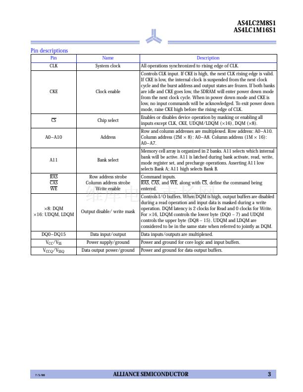
Pin designation
Pin(s)
DQM (2M 脳 8)
UDQM/LDQM (1M 脳 16)
A0 to A10
A11
DQ0 to DQ7 (2M
脳
8)
DQ0 to DQ15 (1M
脳
16)
RAS
CAS
WE
CS
V
CC
, V
CCQ
V
SS
, V
SSQ
CLK
CKE
Description
Output disable/write mask
RA0 鈥?10
Address inputs CA0 鈥?7 (
脳
16)
CA0 鈥?8 (
脳
8)
Bank address (BA)
Input/output
Row address strobe
Column address strobe
Write enable
Chip select
Power (3.3V 鹵 0.3V)
Ground
Clock input
Clock enable
AS4LC2M8S0
LEGEND
Configuration
Refresh Count
Row Address
Bank Address
Column Address
2M
脳
8
1M
脳
8
脳
2 banks
2K
2K (A0 鈥?A10)
2 (BA)
512 (A0 鈥?A8)
1M
脳
16
512K
脳
16
脳
2 banks
2K
2K (A0 鈥?A10)
2 (BA)
256 (A0 鈥?A7)
Selection guide
Symbol
Bus frequency (CL = 3)
Maximum clock access time (CL = 3)
Minimum input setup time
Minimum input hold time
Row cycle time (CL = 3, BL = 1)
Maximum operating current ([
脳
16], RD or
WR, CL = 3), BL = 2
Maximum CMOS standby current, self refresh
7/5/00
鈥?
143
5.5
2
1.0
70
130
1
鈥?
125
6
2
1.0
80
100
1
鈥?0
100
6
2
1.0
80
100
1
Unit
MHz
ns
ns
ns
ns
mA
mA
f
Max
t
AC
t
S
t
H
t
RC
I
CC1
I
CC6
ALLIANCE SEMICONDUCTOR
1
Copyright 漏2000 Alliance Semiconductor. All rights reserved.


 1
1
 2
2
 3
3
 4
4
 5
5
 6
6
 7
7
 8
8
 9
9
 10
10
 11
11
 12
12
 13
13
 14
14
 15
15
 16
16
 17
17
 18
18
 19
19
 20
20
 21
21
 22
22
 23
23
 24
24
 25
25
 26
26
 27
27
 28
28
