March 2001
廬
AS4C4M4FOQ
AS4C4M4F1Q
5V 4M X 4 CMOS QuadCAS DRAM (fastpage mode)
Features
鈥?Organization: 4,194,304 words 脳 4 bits
鈥?High speed
- 50/60 ns RAS access time
- 25/30 ns column address access time
- 12/15 ns CAS access time
鈥?Low power consumption
- Active: 495 mW max
- Standby: 5.5 mW max, CMOS I/O
鈥?Fast page mode
鈥?Refresh
- 4096 refresh cycles, 64 ms refresh interval for
4C4M4FOQ
- 2048 refresh cycles, 32 ms refresh interval for
AS4C4M4F1Q
- RAS-only or CAS-before-RAS refresh or self-refresh
鈥?TTL-compatible, three-state I/O
鈥?4 separate CAS pins allow for separate I/O operation
鈥?JEDEC standard package
- 300 mil, 28-pin SOJ
- 300 mil, 28-pin TSOP
鈥?Latch-up current
鈮?/div>
200 mA
鈥?ESD protection
鈮?/div>
2000 mV
Pin arrangement
SOJ
V
CC
I/O0
I/O1
WE
RAS
*NC/A11
CAS0
CAS1
A10
A0
A1
A2
A3
V
CC
1
2
3
4
5
6
7
8
9
10
11
12
13
14
28
27
26
25
24
23
22
21
20
19
18
17
16
15
GND
I/O3
I/O2
CAS3
OE
A9
CAS2
NC
A8
A7
A6
A5
A4
GND
V
CC
I/O0
I/O1
WE
RAS
*NC/A11
CAS0
CAS1
A10
A0
A1
A2
A3
V
CC
1
2
3
4
5
6
7
8
9
10
Pin designation
TSOP
28
27
26
25
24
23
22
21
20
19
18
17
16
15
GND
I/O3
I/O2
CAS3
OE
A9
CAS2
NC
A8
A7
A6
A5
A4
GND
Pin(s)
A0 to A11
RAS
CAS0 to CAS3
WE
I/O0 to I/O3
OE
V
CC
GND
Description
Address inputs
Row address strobe
Column address strobe
Write enable
Input/output
Output enable
Power
Ground
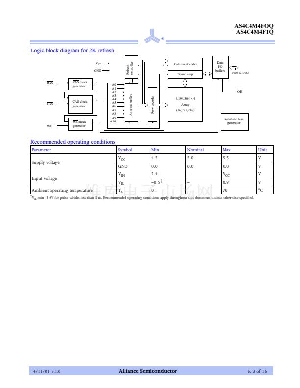
AS4C4M4F0Q/F1Q
11
12
13
14
* NC on 2K refresh version; A11 on 4K refresh version
Selection guide
Symbol
Maximum RAS access time
Maximum column address access time
Maximum CAS access time
Maximum output enable (OE) access time
Minimum read or write cycle time
Minimum fast page mode cycle time
Maximum operating current
Maximum CMOS standby current
4/11/01; v.1.0
AS4C4M4F0Q/1Q
4C4M4FOQ-50
AS4C4M4F1Q-50
50
25
12
13
85
20
90
1.0
4C4M4FOQ-60
AS4C4M4F1Q-60
60
30
15
15
100
24
80
1.0
Unit
ns
ns
ns
ns
ns
ns
mA
mA
P. 1 of 16
t
RAC
t
CAA
t
CAC
t
OEA
t
RC
t
PC
I
CC1
I
CC5
Alliance Semiconductor
Copyright 漏 Alliance Semiconductor. All rights reserved.


 1
1
 2
2
 3
3
 4
4
 5
5
 6
6
 7
7
 8
8
 9
9
 10
10
 11
11
 12
12
 13
13
 14
14
 15
15
 16
16
