PRELIMINARY TECHNICAL DATA
a
Preliminary Technical Data
FEATURES
256 Position
AD5280 鈥?1-Channel
AD5282 鈥?2-Channel (Independently Programmable)
Potentiometer Replacement
20K, 50K, 200K Ohm with TC < 50ppm/潞C
Internal Power ON Mid-Scale Preset
+5 to +15V Single-Supply; 鹵5.5V Dual-Supply Operation
I
2
C Compatible Interface
APPLICATIONS
Multi-Media, Video & Audio
Communications
Mechanical Potentiometer Replacement
Instrumentation: Gain, Offset Adjustment
Programmable Voltage to Current Conversion
Line Impedance Matching
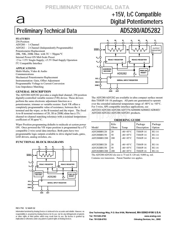
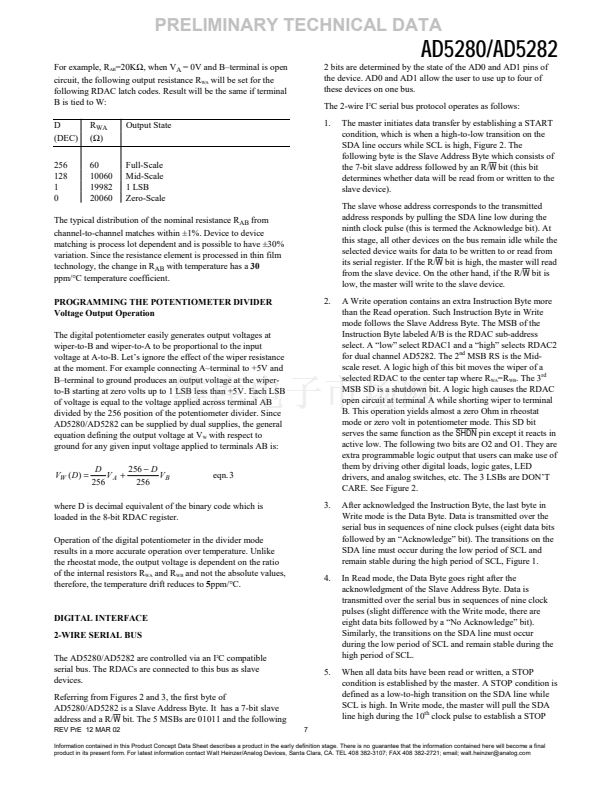
A
1
SHDN
V
DD
+15V, I
2
C Compatible
Digital Potentiometers
AD5280/AD5282
W
1
B
1
A
2
W
2
B
2
O
1
OUTPUT
REGISTER
R
RDAC1 REGISTER
V
SS
V
L
ADDRESS
DECODE
R
RDAC2 REGISTER
R
AD5282
SCL
SDA
GND
PWR ON
RESET
8
SERIAL INPUT REGISTER
GENERAL DESCRIPTION
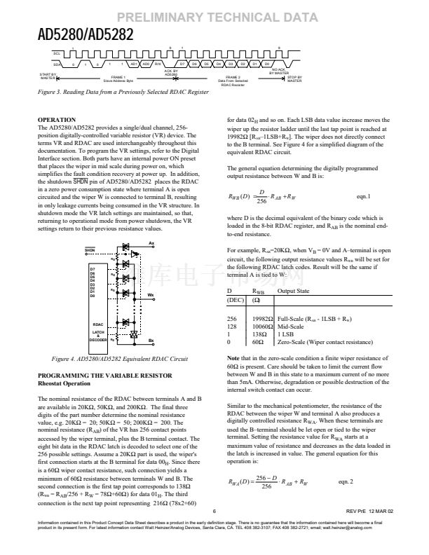
The AD5280/AD5282 provides a single/dual channel, 256 position
digitally-controlled variable resistor (VR) device. These devices
perform the same electronic adjustment function as a
potentiometer, trimmer or variable resistor. Each VR offers a
completely programmable value of resistance, between the A
terminal and the wiper, or the B terminal and the wiper. The fixed
A-to-B terminal resistance of 20, 50 or 200K ohms has a 1%
channel-to-channel matching tolerance with a nominal temperature
coefficient of 30 ppm/擄C.
Wiper Position programming defaults to midscale at system power
ON. Once powered the VR wiper position is programmed by a I
2
C
compatible 2-wire serial data interface. Both parts have two
programmable logic outputs available to drive digital loads, gates,
LED drivers, analog switches, etc.
AD0
AD1
The AD5280/AD5282 are available in ultra compact surface mount
thin TSSOP-14/-16 packages. All parts are guaranteed to operate
over the extended industrial temperature range of -40擄C to +85擄C.
For 3-wire, SPI compatible interface applications, see
AD5203/AD5204/AD5206/AD7376/AD8400/AD8402/AD8403/
AD5260/AD5262/AD5200/AD5201 products.
ORDERING GUIDE
Model
AD5280BRU20
AD5280BRU50
AD5280BRU200
AD5282BRU20
AD5282BRU50
AD5282BRU200
Kilo
Ohms
20
50
200
20
50
200
Temp
-40/+85擄C
-40/+85擄C
-40/+85擄C
-40/+85擄C
-40/+85擄C
-40/+85擄C
Package
Description
TSSOP-14
TSSOP-14
TSSOP-14
TSSOP-16
TSSOP-16
TSSOP-16
Package
Option
RU-14
RU-14
RU-14
RU-16
RU-16
RU-16
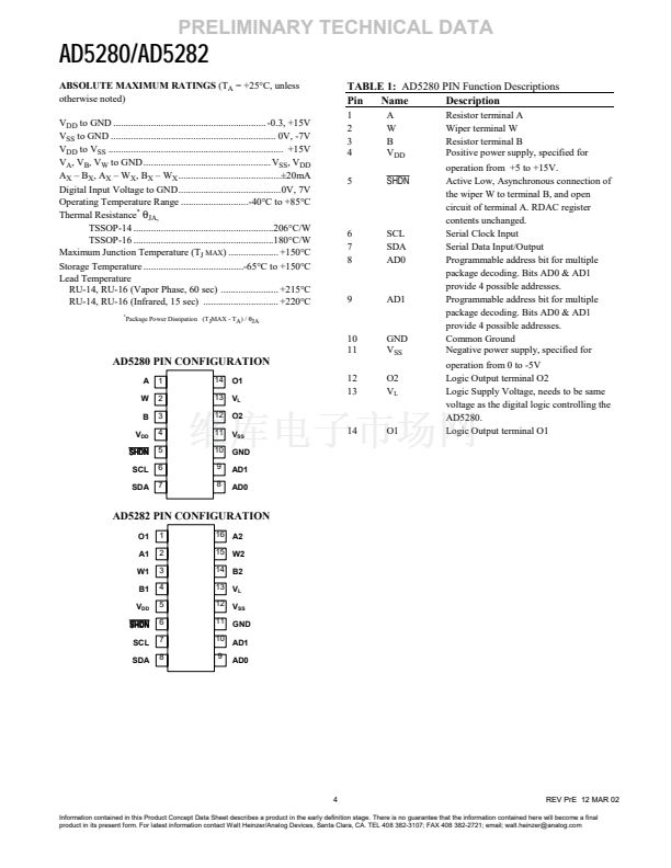
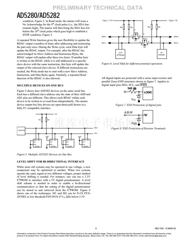
FUNCTIONAL BLOCK DIAGRAMS
A
1
W
1
B
1
O
1
O
2
SHDN
The AD5280/AD5282 die size is 75 mil X 120 mil, 9,000 sq. mil.
Contains xxx transistors. Patent Number xxx applies.
RDAC1 REGISTER
RDAC2 REGISTER
R
V
DD
V
SS
V
L
ADDRESS
DECODE
PWR ON
RESET
8
R
AD5280
SCL
SDA
GND
SERIAL INPUT REGISTER
AD0
AD1
REV PrE 12 MAR 02
Information furnished by Analog Devices is believed to be accurate and reliable. However, no
responsibility is assumed by Analog Devices for its use; nor for any infringements of patents
or other rights of third parties which may result from its use. No license is granted by
implication or otherwise under any patent or patent rights of Analog Devices.
One Technology Way, P.O. Box 9106,
Norwood, MA 02062-9106 U
.
S
.
A
.
Tel: 781/329-4700
Fax: 781/326-8703
www.analog.com
漏Analog Devices, Inc., 2002


 1
1
 2
2
 3
3
 4
4
 5
5
 6
6
 7
7
 8
8
 9
9
 10
10
