危鈭?/div>
11,12,13
DRIVER
HIGH SIDE
DRIVER
LOW SIDE
LEVEL
SHIFT
+
DEAD
TIME
CONTROL
DRIVER
LOW SIDE
PGND2
PVDD2
46,47,48
PGND2
39,40
DRIVER
HIGH SIDE
DRIVER
LOW SIDE
PVDD2
36,37,38
OUTR-
PGND1
PGND2
33,34,35
14,15,16
PGND1
PGND2
REF_FILT
AVDD
55
脴1
VOLTAGE
REFERENCE
脴2
脴1
脴2
57
56
AGND
DVDD
DGND
24,25
23,26
TEMPERATURE
SENSE &
OVER-CURRENT
PROTECTION
OSCILLATOR
MODE CONTROL LOGIC
MUTE/
POP
CONTROL
27
RST/PW DN
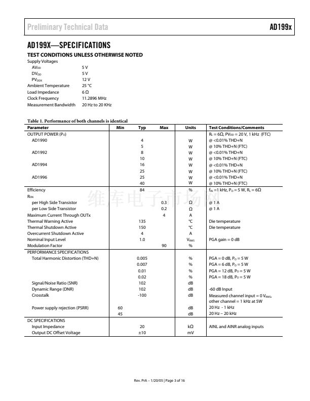
Figure 1. Block Diagram
Rev. PrA 鈥?1/20/05
Information furnished by Analog Devices is believed to be accurate and reliable.
However, no responsibility is assumed by Analog Devices for its use, nor for any
infringements of patents or other rights of third parties that may result from its use.
Specifications subject to change without notice. No license is granted by implication
or otherwise under any patent or patent rights of Analog Devices. Trademarks and
registered trademarks are the property of their respective companies.
One Technology Way, P.O. Box 9106, Norwood, MA 02062-9106, U.S.A.
www.analog.com
Tel: 781.329.4700
Fax: 781.326.8703
漏 2005 Analog Devices, Inc. All rights reserved.
DCTRL0
DCTRL1
DCTRL2
ERR0
ERR1
MUTE
ERR2
MONO
CLKI
28
30
29
19
18
17
49
22
21
20
CLKO


 1
1
 2
2
 3
3
 4
4
 5
5
 6
6
 7
7
 8
8
 9
9
 10
10
 11
11
 12
12
 13
13
 14
14
 15
15
 16
16
