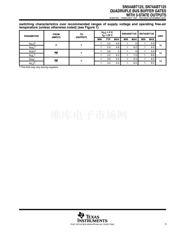
SN54ABT125, SN74ABT125
QUADRUPLE BUS BUFFER GATES
WITH 3-STATE OUTPUTS
SCBS182I 鈥?FEBRUARY 1997 鈥?REVISED NOVEMBER 2002
D
D
D
Typical V
OLP
(Output Ground Bounce)
<1 V at V
CC
= 5 V, T
A
= 25擄C
High-Drive Outputs (鈥?2-mA I
OH
, 64-mA I
OL
)
I
off
and Power-Up 3-State Support Hot
Insertion
D
D
Latch-Up Performance Exceeds 500 mA Per
JEDEC Standard JESD-17
ESD Protection Exceeds JESD 22
鈥?2000-V Human-Body Model (A114-A)
鈥?200-V Machine Model (A115-A)
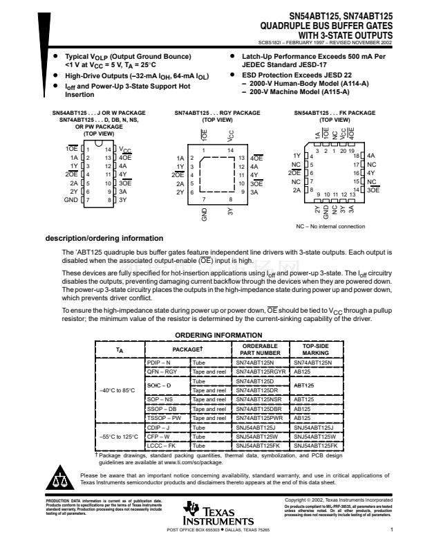
SN54ABT125 . . . FK PACKAGE
(TOP VIEW)
1OE
1OE
1A
1Y
2OE
2A
2Y
GND
1
2
3
4
5
6
7
14
13
12
11
10
9
8
V
CC
4OE
4A
4Y
3OE
3A
3Y
1
14
13
12
11
10
9
V
CC
1A
1Y
2OE
2A
2Y
2
3
4
5
6
7
8
4OE
4A
4Y
3OE
3A
1Y
NC
2OE
NC
2A
1A
1OE
NC
V
CC
4OE
4
5
6
7
8
3 2 1 20 19
18
17
16
15
14
9 10 11 12 13
SN54ABT125 . . . J OR W PACKAGE
SN74ABT125 . . . D, DB, N, NS,
OR PW PACKAGE
(TOP VIEW)
SN74ABT125 . . . RGY PACKAGE
(TOP VIEW)
4A
NC
4Y
NC
3OE
GND
NC 鈥?No internal connection
description/ordering information
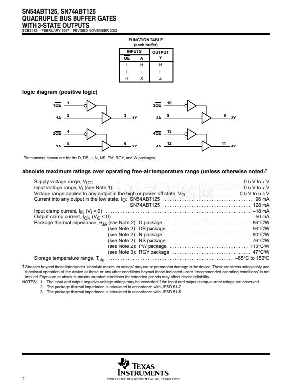
The 鈥橝BT125 quadruple bus buffer gates feature independent line drivers with 3-state outputs. Each output is
disabled when the associated output-enable (OE) input is high.
These devices are fully specified for hot-insertion applications using I
off
and power-up 3-state. The I
off
circuitry
disables the outputs, preventing damaging current backflow through the devices when they are powered down.
The power-up 3-state circuitry places the outputs in the high-impedance state during power up and power down,
which prevents driver conflict.
To ensure the high-impedance state during power up or power down, OE should be tied to V
CC
through a pullup
resistor; the minimum value of the resistor is determined by the current-sinking capability of the driver.
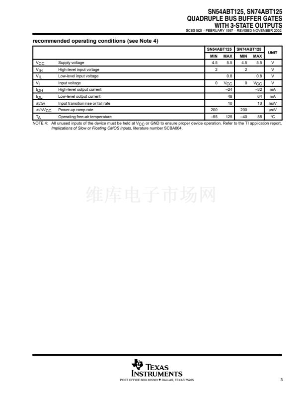
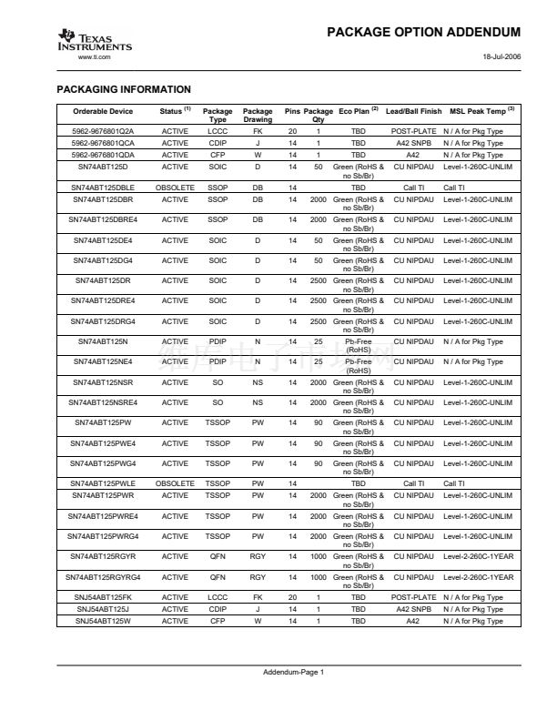
ORDERING INFORMATION
TA
PDIP 鈥?N
QFN 鈥?RGY
鈥?0擄C to 85擄C
SOIC 鈥?D
SOP 鈥?NS
SSOP 鈥?DB
TSSOP 鈥?PW
CDIP 鈥?J
鈥?5擄C to 125擄C
CFP 鈥?W
LCCC 鈥?FK
PACKAGE鈥?/div>
Tube
Tape and reel
Tube
Tape and reel
Tape and reel
Tape and reel
Tape and reel
Tube
Tube
Tube
ORDERABLE
PART NUMBER
SN74ABT125N
SN74ABT125RGYR
SN74ABT125D
SN74ABT125DR
SN74ABT125NSR
SN74ABT125DBR
SN74ABT125PWR
SNJ54ABT125J
SNJ54ABT125W
SNJ54ABT125FK
TOP-SIDE
MARKING
SN74ABT125N
AB125
ABT125
ABT125
AB125
AB125
SNJ54ABT125J
SNJ54ABT125W
SNJ54ABT125FK
鈥?Package drawings, standard packing quantities, thermal data, symbolization, and PCB design
guidelines are available at www.ti.com/sc/package.
Please be aware that an important notice concerning availability, standard warranty, and use in critical applications of
Texas Instruments semiconductor products and disclaimers thereto appears at the end of this data sheet.
Copyright
錚?/div>
2002, Texas Instruments Incorporated
On products compliant to MIL-PRF-38535, all parameters are tested
unless otherwise noted. On all other products, production
processing does not necessarily include testing of all parameters.
PRODUCTION DATA information is current as of publication date.
Products conform to specifications per the terms of Texas Instruments
standard warranty. Production processing does not necessarily include
testing of all parameters.
POST OFFICE BOX 655303
鈥?/div>
DALLAS, TEXAS 75265
2Y
GND
NC
3Y
3A
3Y
1


 1
1
 2
2
 3
3
 4
4
 5
5
 6
6
 7
7
 8
8
 9
9
 10
10
 11
11
 12
12
 13
13
 14
14
 15
15
 16
16
 17
17
 18
18
 19
19
 20
20
