廬
APPLICATION BULLETIN
By Christian Henn, and Ernst Rau, Burr-Brown International GmbH
Mailing Address: PO Box 11400 鈥?Tucson, AZ 85734 鈥?Street Address: 6730 S. Tucson Blvd. 鈥?Tucson, AZ 85706
Tel: (602) 746-1111 鈥?Twx: 910-952-111 鈥?Telex: 066-6491 鈥?FAX (602) 889-1510 鈥?Immediate Product Info: (800) 548-6132
THERE鈥橲 A WORLD OF LINE DRIVERS TO CHOOSE FROM
Coax cables with a typical impedance of 50鈩?or 75鈩?are
used in many applications to ensure signal fidelity, and high-
speed line drivers have the often difficult job of transmitting
signals over these cables or over twisted pair lines. The most
common way to drive coax cables is to use driver amplifiers
with low-impedance voltage output, which operate with
either voltage or current feedback. Now, however, the
wideband OTAs, OPA660 and OPA2662, offer a high-
impedance current output, giving engineers more flexibility
and more options. Since both voltage and current outputs
have their advantages and disadvantages, engineers can
choose the method that provides the best compromise for
their applications.
direct-feedback configuration. One special feature of the
OPA2662 is its ability to switch the EN inputs of the OTAs
independently; the OTAs can be switched on within 30ns
and off within 250ns at maximum output power.
THE BASIC FACTS ABOUT A
LOW-IMPEDANCE TRANSMISSION LINE
The most important equations and technical basics of trans-
mission lines support the results found for the various drive
circuits presented here. An ideal transmission medium with
zero ohmic impedance would have inductance and capaci-
tance distributed over the transmission cable. Both induc-
tance and capacitance detract from the transmission quality
of a line. Each input is connected with high impedance to the
line as in a daisy chain or loop-through configuration, and
each adds capacitance of at least a few picofarad. The typical
transmission line impedance (Z
O
) defines the line type. In
equation (1), the impedance is calculated by the square root
of line inductance (L
T
) divided by line capacitance (C
T
):
1
2
3
4
5
V
IN
R
OUT
Z
O
V
OUT
R
2
R
LOAD
6
R
1
Z
0
=
L
T
C
T
(1)
FIGURE 1. Typical Line Driver Circuit.
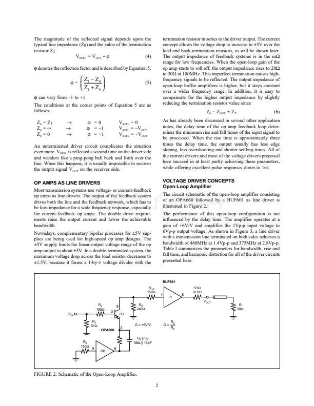
WIDE-BAND OPERATIONAL
AMPLIFIERS OPA660 AND OPA2662
The OPA660 was used in open-loop, direct-feedback, and
current-feedback modes to implement different voltage drive
configurations. The open-loop buffer amplifier, BUF601,
located behind the OPA660 in the circuit, decouples the
high-impedance OTA collector output and provides a low-
impedance voltage source output to drive the transmission
line or bus system. The OPA660 contains the so-called
Diamond Transistor (DT) and a buffer amplifier called the
Diamond Buffer (DB) in an 8-pin plastic package. The
buffer amplifier input is connected to GND in all three
versions and compensates the input offset voltage of the
OTA. As indicated in the PDS, the drive capability of the
BUF601 is
鹵20mA
for continuous current but can easily go
up to
鹵50mA
for pulse applications.
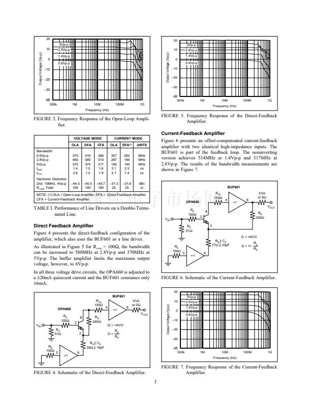
The OPA2662 contains two OTAs in a 16-pin plastic pack-
age; each can deliver output current of
鹵75mA.
By connect-
ing the two collector outputs, it is possible to increase the
current drive capability to
鹵150mA.
For the current drive
concept, the OPA2662 operates in open-loop mode and in a
漏
In the same manner, line inductance and capacitance deter-
mine the delay time of a transmission line as shown in
equation (2):
T
=
L
T
鈥?C
T
(2)
Typical values for Z
O
are 240鈩?for symmetrical lines and
75鈩?or 50鈩?for coax cables. Z
O
sometimes decreases to 30鈩?/div>
to 40鈩?in high data rate bus systems for bus lines on printed
circuit boards. In general, the more complex a bus system is,
the lower Z
O
will be. Because it increases the capacitance of
the transmission medium, a complex system lowers the
typical line impedance, resulting in higher drive require-
ments for the line drivers used here.
Transmission lines are almost always terminated on the
transmitter line and always terminated on the receiver side.
Unterminated lines generate signal reflections that degrade
the pulse fidelity. The driver circuit transmits the output
voltage (V
OUT
) over the line. The signal appears at the end of
the line and will be reflected when not properly terminated.
The reflected portion of V
OUT
, called V
REFL
, returns to the
driver. The transmitted signal is the sum of the original
signal V
OUT
and the reflected V
REFL
.
V
T
= V
OUT
+ V
REFL
(3)
1993 Burr-Brown Corporation
AB-191
Printed in U.S.A. November, 1993


 1
1
 2
2
 3
3
 4
4
 5
5
