廬
APPLICATION BULLETIN
Mailing Address: PO Box 11400 鈥?Tucson, AZ 85734 鈥?Street Address: 6730 S. Tucson Blvd. 鈥?Tucson, AZ 85706
Tel: (602) 746-1111 鈥?Twx: 910-952-111 鈥?Telex: 066-6491 鈥?FAX (602) 889-1510 鈥?Immediate Product Info: (800) 548-6132
BUILDING A 400MHz WIDE-BAND DIFFERENTIAL AMPLIFIER:
IT'S A BREEZE WITH THE DIAMOND TRANSISTOR OPA660.
By Christian Henn and Ernst Rau, Burr-Brown International GmbH
In radio frequency (RF) technology, signals from oscillo-
scopes, monitors, transient recorders, and many other de-
vices are usually connected to sensors and generators via
coaxial lines. In any transmission, however, interference
voltages caused by differences in potential between the
sender and receiver and by electromagnetic interference
distort the results, particularly when the signals being trans-
mitted are sensitive and wide-band. Designers of this type of
transmission system need shielded, symmetrical transmis-
sion lines and input differential amplifiers with high com-
mon-mode rejection, which bring home the signals without
humming or radio interference.
Designing this type of differential amplifier used to be quite
a chore, involving extensive and complicated hardware. But
the development of new, monolithic ICs such as the Dia-
mond Transistor OPA660 has changed all that. The OPA660
makes it easy to design a 400MHz differential amplifier
offering 鈥?0dB common-mode rejection at a 1MHz fre-
quency. This amplifier uses an open-loop amplifier structure
with two identical high-impedance inputs and no feedback.
The parameters such as wide bandwidth, stable operation,
and excellent pulse processing, common-mode rejection,
and harmonic distortion let the performance speak for itself.
BASIC TRANSMISSION STRUCTURES
Figure 1 shows a symmetrical transmission path with signal
voltage V
S
and cable termination resistors R
IN
and R
t
. A
symmetrical voltage source normally uses amplifiers with
complementary outputs or transformers to balance or adapt
the circuits. The relatively high-impedance input resistor R
b
limits the input potential drift through the input bias currents
(I
BIAS
), and the symmetrical differential amplifier input re-
jects interference voltages superimposed upon the input
signal and its reference potential. The voltage-controlled
current source converts the symmetrical input voltage V
IN
either into an output current or into the asymmetrical output
voltage V
OUT
when a voltage drop is present at the external
resistor R
OUT
. V
IN
and V
OUT
are related as follows: V
OUT
= V
IN
鈥?gm 鈥?R
OUT
, where gm is the transconductance of the
operational transconductance amplifier (OTA). The buffer
following the input amplifier decouples the low-impedance
load resistor from the high-impedance OTA output.
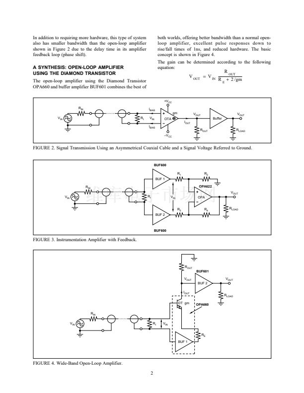
Instead of symmetrical signal excitation, many applications
use the type of transmission path shown in Figure 2. A
single-ended signal voltage V
IN
drives an asymmetrical
coaxial cable terminated on both sides. In this structure as
well, the symmetrical differential amplifier input rejects
interference voltages superimposed on the signal.
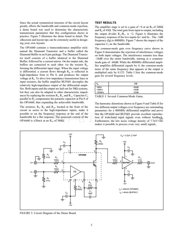
INSTRUMENTATION AMPLIFIER WITH FEEDBACK
OTAs and buffers have conventionally been designed using
differential amplifiers as shown in Figure 3. The feedback
path from the op amp output over R
4
generates a relatively
low-impedance inverting input, which is equal to the R
3
resistor value. Inserting the buffer amplifier, BUF2, converts
the low-impedance input to high impedance, while inserting
the buffer amplifier, BUF1, optimizes the input symmetry
and thus the common-mode rejection at DC and vs fre-
quency.
The gain is R
4
/R
3
during signal excitation at the inverting
input and 1 + R
4
/R
3
during signal excitation at the noninverting
input. A divider is inserted between R
1
and R
2
to compensate
for these differing gains. Buffer 1 also synchronizes the
signal delay times of the two inputs, which is important for
good common-mode rejection at high frequencies. To achieve
high common-mode rejection over frequency, it is important
that the gain curve of the two input buffers be as identical as
possible.
+V
CC
R
IN
V
IN
R
t
I
BIAS
gm
V
IN
I
BIAS
R
b
鈥揤
CC
OTA
I
OUT
R
OUT
R
LOAD
V
OUT
Buffer
V
OUT
1
2
3
4
5
6
FIGURE 1. Basic Structure of a Symmetrical Transmission Path.
漏
1993 Burr-Brown Corporation
AN-188
Printed in U.S.A. November, 1993


 1
1
 2
2
 3
3
 4
4
