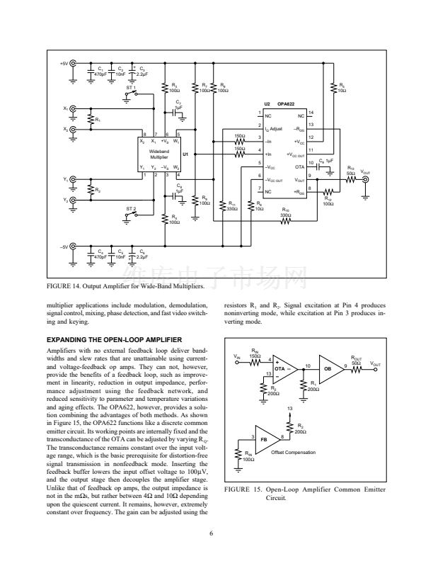
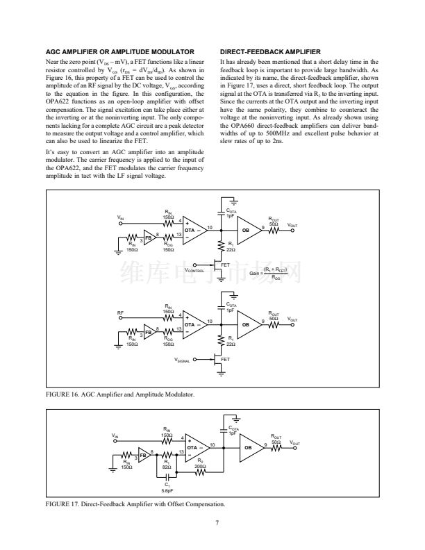
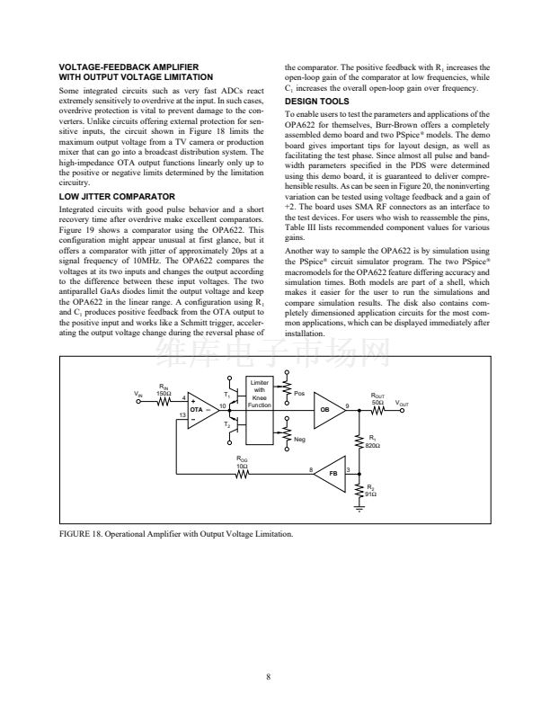
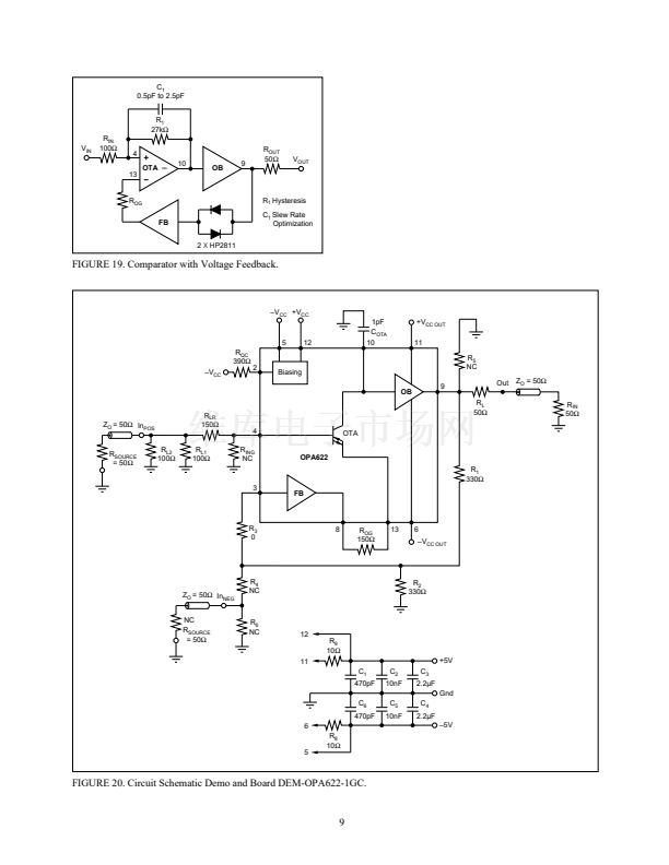
APPLICATION NOTE
Mailing Address: PO Box 11400 鈥?Tucson, AZ 85734 鈥?Street Address: 6730 S. Tucson Blvd. 鈥?Tucson, AZ 85706
Tel: (602) 746-1111 鈥?Twx: 910-952-1111 鈥?Telex: 066-6491 鈥?FAX: (602) 889-1510 鈥?Immediate Product Info: (800) 548-6132
CURRENT OR VOLTAGE FEEDBACK:
THE CHOICE IS YOURS WITH THE NEW, FLEXIBLE,
WIDE-BAND OPERATIONAL AMPLIFIER OPA622.
By Christian Henn and Andreas Sibrai, Burr-Brown International GmbH
With the recently introduced wide-band op amp OPA622,
Burr-Brown has reached a new height in op amp design. In
the past, engineers designing a circuit with feedback had to
choose between voltage and current feedback according to
the requirements of their particular applications. Both feed-
back types involve a trade-off. The current-feedback struc-
tures available up to now use their symmetrical circuit
design and short feedback loop to process wide-band analog
signals, while the traditional voltage-feedback amplifiers
provide more optimized DC performance but slow down the
signal processing rate. But with the OPA622, an IC is
available that can be configured for both modes. The first
voltage-feedback op amp manufactured using a complemen-
tary circuit technique, the OPA622 achieves bandwidths and
slew rates previously attainable only with current-feedback
amplifiers, while also offering two identical high-impedance
inputs, improved common-mode rejection, and external ad-
justment of the open-loop gain and quiescent current. The
OPA622鈥檚 extremely flexible pin configuration lets the user
assemble it as a voltage-feedback op amp, a fast comparator,
an AGC amplifier, an open-loop or direct-feedback ampli-
fier, and even a 350MHz current-feedback amplifier. Its
powerful output stage can easily drive 50鈩?and 75鈩?trans-
mission systems and operates stably on capacitive load
resistors. This application note will present the internal
circuit configuration, specifications, and frequency response
alignment of the OPA622 and will also describe its diverse
applications.
CLASSICAL CIRCUIT TECHNIQUES
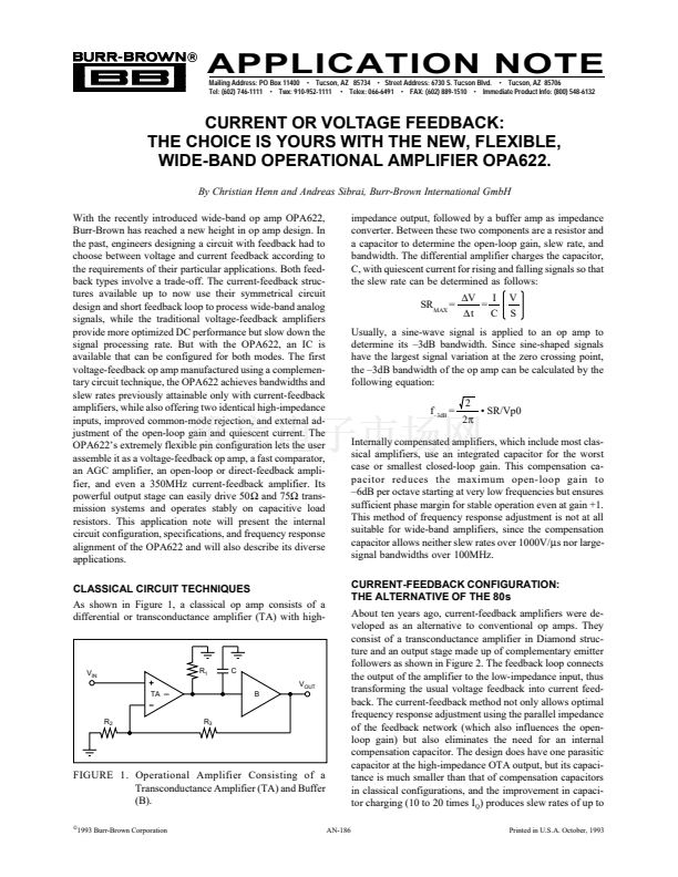
As shown in Figure 1, a classical op amp consists of a
differential or transconductance amplifier (TA) with high-
impedance output, followed by a buffer amp as impedance
converter. Between these two components are a resistor and
a capacitor to determine the open-loop gain, slew rate, and
bandwidth. The differential amplifier charges the capacitor,
C, with quiescent current for rising and falling signals so that
the slew rate can be determined as follows:
SR
MAX
=
鈭哣
I
=
鈭唗
C
V
S
Usually, a sine-wave signal is applied to an op amp to
determine its 鈥?dB bandwidth. Since sine-shaped signals
have the largest signal variation at the zero crossing point,
the 鈥?dB bandwidth of the op amp can be calculated by the
following equation:
f
鈥?dB
=
2
2蟺
鈥?SR/Vp0
Internally compensated amplifiers, which include most clas-
sical amplifiers, use an integrated capacitor for the worst
case or smallest closed-loop gain. This compensation ca-
pacitor reduces the maximum open-loop gain to
鈥?dB per octave starting at very low frequencies but ensures
sufficient phase margin for stable operation even at gain +1.
This method of frequency response adjustment is not at all
suitable for wide-band amplifiers, since the compensation
capacitor allows neither slew rates over 1000V/碌s nor large-
signal bandwidths over 100MHz.
CURRENT-FEEDBACK CONFIGURATION:
THE ALTERNATIVE OF THE 80s
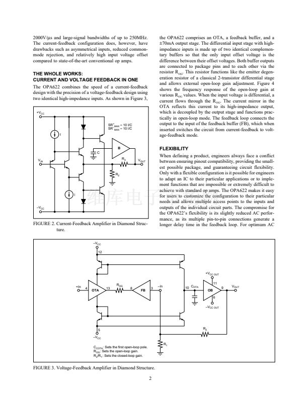
About ten years ago, current-feedback amplifiers were de-
veloped as an alternative to conventional op amps. They
consist of a transconductance amplifier in Diamond struc-
ture and an output stage made up of complementary emitter
followers as shown in Figure 2. The feedback loop connects
the output of the amplifier to the low-impedance input, thus
transforming the usual voltage feedback into current feed-
back. The current-feedback method not only allows optimal
frequency response adjustment using the parallel impedance
of the feedback network (which also influences the open-
loop gain) but also eliminates the need for an internal
compensation capacitor. The design does have one parasitic
capacitor at the high-impedance OTA output, but its capaci-
tance is much smaller than that of compensation capacitors
in classical configurations, and the improvement in capaci-
tor charging (10 to 20 times I
Q
) produces slew rates of up to
AN-186
Printed in U.S.A. October, 1993
V
IN
TA
鈭?/div>
R
1
C
V
OUT
B
R
2
R
3
FIGURE 1. Operational Amplifier Consisting of a
Transconductance Amplifier (TA) and Buffer
(B).
漏
1993 Burr-Brown Corporation


 1
1
 2
2
 3
3
 4
4
 5
5
 6
6
 7
7
 8
8
 9
9
 10
10
