廬
APPLICATION BULLETIN
DIAMOND TRANSISTOR OPA660
By Klaus Lehmann, Burr-Brown International GmbH
Mailing Address: PO Box 11400 鈥?Tucson, AZ 85734 鈥?Street Address: 6730 S. Tucson Blvd. 鈥?Tucson, AZ 85706
Tel: (602) 746-1111 鈥?Twx: 910-952-111 鈥?Telex: 066-6491 鈥?FAX (602) 889-1510 鈥?Immediate Product Info: (800) 548-6132
CIRCUIT TECHNOLOGY WITH
THE DIAMOND TRANSISTOR OPA660
The monolithic integrated circuit OPA660 uses the Dia-
mond structure to act as an ideal transistor. However, this
circuit has the advantage that it avoids the biasing circuits
and eliminates the need for an offset voltage compensation
network. With this element, peripheral components are re-
duced to the essential minimum. Using the DC-coupled
wideband voltage amplifier and buffer, conventional and
new circuit designs of the OPA660 can be compared with
each other.
A report in Electronik Industrie 90 (vol. 1, p.70) presented
basic explanations, along with a schematic overview of
circuits possible with the voltage-controlled current source
OPA660. This article is intended to describe the practical
circuit design. From the many possible application circuits,
this article first examines the basic circuits without external
feedback.
DIAMOND TRANSISTOR
Figure 1 illustrates what is probably the simplest DC-
coupled voltage amplifier. Several factors in the circuit
design are disadvantageous for easy and general application:
the input offset voltage which is dependent upon tempera-
ture (V
IO
= 鈥?27mV鈥攕ee Table I), the output offset volt-
age鈥?also dependent upon the temperature (V
OO
= + 3V),
and the bias current (I
O
= 2mA), which flows through the
output load resistor (1k鈩?. When the offset-free signal
voltage V
IN
appears at the output, it is amplified as desired
(G = 2) but is superimposed with bias voltage and current.
These DC currents and bias voltages, which are determined
by the transistor, are systematically compensated in the
following circuit variations. V
IO
and I
O
require that the
emitter resistor be divided (743鈩?and 1.53k鈩?. The signal
voltage gain results from:
G=
V
OUT
V
IN
鈮?/div>
1k鈩?/div>
=2
743||1.53k鈩?/div>
+5V
1.11k鈩?/div>
2mA
630鈩?/div>
V
OUT
V
IN
2.42k鈩?/div>
10k鈩?/div>
鈥?V
FIGURE 2. Adjustment of V
IO
.
+5V
1k鈩?/div>
V
OUT
V
IN
Further important parameters are summarized in Table I. In
Figure 2, V
IO
is compensated with a previously inserted
complementary emitter follower (pnp), while V
OO
is com-
pensated with a zener diode inserted afterward. I
O
still
requires division of the emitter resistor (630鈩?and 2.42k鈩?.
The signal gain now results from:
G=
V
OUT
V
IN
鈮?/div>
(1.11k鈩?|| 10k鈩?/(630鈩?|| 2.42k鈩? = 2
2mA
743鈩?/div>
1.53k鈩?/div>
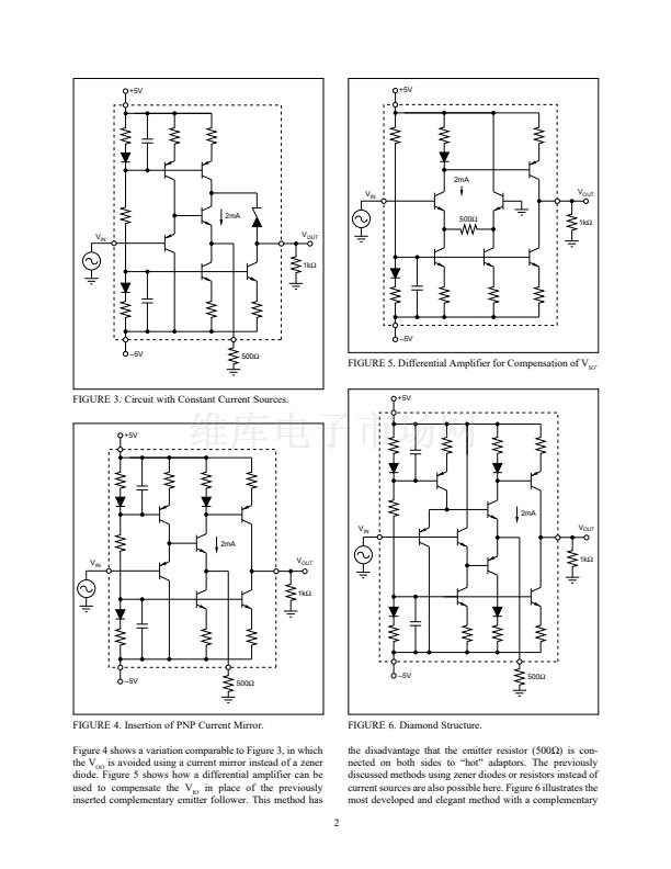
With current sources as shown in Figure 3, the gain deter-
mined by the resistors (500鈩?and 1k鈩? can be achieved as
desired, without bias currents and voltages.
G=
V
OUT
V
IN
鈮?/div>
1k鈩?/div>
=2
500鈩?/div>
鈥?V
FIGURE 1. DC-Coupled Voltage Amplifier.
漏
1993 Burr-Brown Corporation
AB-181
Printed in U.S.A. May, 1993
AB-181相關(guān)型號(hào)PDF文件下載
-
型號(hào)
版本
描述
廠商
下載
-
英文版
Application Bulletin AB-12
FAIRCHILD
-
英文版
Application Bulletin AB-12
FAIRCHILD ...
-
英文版
AB-100 - MULTIPLEXER DATA ACQUISTION SYSTEM
ETC
-
英文版
AB-101 - COMBINING AN AMPLIFIER WITH THE BUF634
ETC
-
英文版
AB-102 - OUTPUT SPECTRUM AND POST-LPF DESIGN OF THE PCM1710
ETC
-
英文版
AB-103 - NOISE ANALYSIS FOR HIGH SPEED OP AMPS
ETC
-
英文版
ETC
-
英文版
AB-105 - TUNING IN AMPLIFIERS
ETC
-
英文版
AB-106 - PROGRAMMING TRICKS FOR HIGHER CONVERSION SPEEDS UTI...
ETC
-
英文版
AB-107 - GIVING CONVERTERS A LITTLE GAIN BOOST WITH A FRONT ...
ETC
-
英文版
AB-109 - ADS7809 TAG FEATURE
ETC
-
英文版
AB-110 - VOLTAGE REFERENCE SCALING TECHNIQUES Increase the A...
ETC
-
英文版
AB-111 - DEM-ADS1210
ETC
-
英文版
ETC
-
英文版
AB-113 - ACCESSING THE ADS1210 DEMO BOARD WITH YOUR PC
ETC
-
英文版
AB-115 - OVERDRIVING THE INPUTS TO THE ADS1210. ADS1211. ADS...
ETC
-
英文版
ETC
-
英文版
ETC
-
英文版
AB-118 - EXTRACT AND DIGITIZE AC SIGNALS WITH A SINGLE A
ETC
-
英文版
"AB-119 - A ""GETTING STARTED"" GUIDE FOR THE CONVERTER...
ETC


 1
1
 2
2
 3
3
 4
4
 5
5
 6
6
 7
7
