廬
APPLICATION BULLETIN
ULTRA HIGH-SPEED ICs
By Klaus Lehmann, Burr-Brown International GmbH
Mailing Address: PO Box 11400 鈥?Tucson, AZ 85734 鈥?Street Address: 6730 S. Tucson Blvd. 鈥?Tucson, AZ 85706
Tel: (602) 746-1111 鈥?Twx: 910-952-111 鈥?Telex: 066-6491 鈥?FAX (602) 889-1510 鈥?Immediate Product Info: (800) 548-6132
1
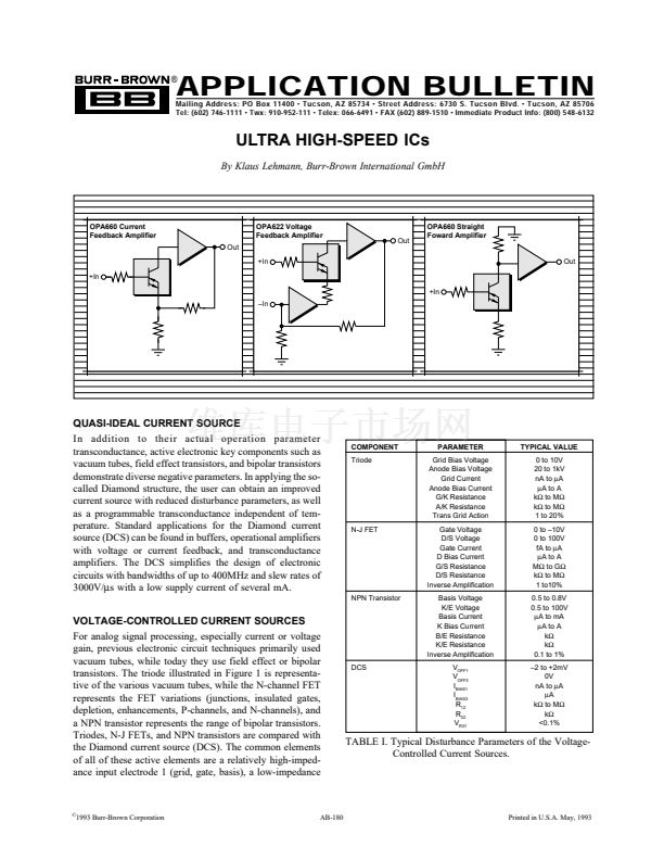
OPA660 Current
Feedback Amplifier
Out
+In
+In
+In
鈥揑n
OPA622 Voltage
Feedback Amplifier
Out
OPA660 Straight
Foward Amplifier
2
Out
3
4
5
QUASI-IDEAL CURRENT SOURCE
In addition to their actual operation parameter
transconductance, active electronic key components such as
vacuum tubes, field effect transistors, and bipolar transistors
demonstrate diverse negative parameters. In applying the so-
called Diamond structure, the user can obtain an improved
current source with reduced disturbance parameters, as well
as a programmable transconductance independent of tem-
perature. Standard applications for the Diamond current
source (DCS) can be found in buffers, operational amplifiers
with voltage or current feedback, and transconductance
amplifiers. The DCS simplifies the design of electronic
circuits with bandwidths of up to 400MHz and slew rates of
3000V/碌s with a low supply current of several mA.
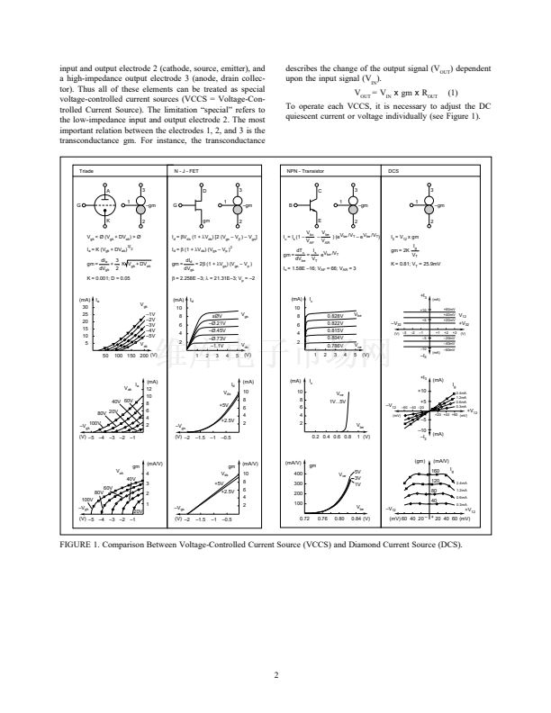
VOLTAGE-CONTROLLED CURRENT SOURCES
For analog signal processing, especially current or voltage
gain, previous electronic circuit techniques primarily used
vacuum tubes, while today they use field effect or bipolar
transistors. The triode illustrated in Figure 1 is representa-
tive of the various vacuum tubes, while the N-channel FET
represents the FET variations (junctions, insulated gates,
depletion, enhancements, P-channels, and N-channels), and
a NPN transistor represents the range of bipolar transistors.
Triodes, N-J FETs, and NPN transistors are compared with
the Diamond current source (DCS). The common elements
of all of these active elements are a relatively high-imped-
ance input electrode 1 (grid, gate, basis), a low-impedance
6
COMPONENT
Triode
PARAMETER
Grid Bias Voltage
Anode Bias Voltage
Grid Current
Anode Bias Current
G/K Resistance
A/K Resistance
Trans Grid Action
Gate Voltage
D/S Voltage
Gate Current
D Bias Current
G/S Resistance
D/S Resistance
Inverse Amplification
Basis Voltage
K/E Voltage
Basis Current
K Bias Current
B/E Resistance
K/E Resistance
Inverse Amplification
V
OFF1
V
OFF3
I
BIAS1
I
BIAS3
R
12
R
32
V
R31
TYPICAL VALUE
0 to 10V
20 to 1kV
nA to
碌A(chǔ)
碌A(chǔ)
to A
k鈩?to M鈩?/div>
k鈩?to M鈩?/div>
1 to 20%
0 to 鈥?0V
0 to 100V
fA to
碌A(chǔ)
碌A(chǔ)
to A
M鈩?to G鈩?/div>
k鈩?to M鈩?/div>
1 to10%
0.5 to 0.8V
0.5 to 100V
碌A(chǔ)
to mA
碌A(chǔ)
to A
k鈩?/div>
k鈩?/div>
0.1 to 1%
鈥? to +2mV
0V
nA to
碌A(chǔ)
碌A(chǔ)
k鈩?to M鈩?/div>
k鈩?/div>
<0.1%
N-J FET
NPN Transistor
DCS
TABLE I. Typical Disturbance Parameters of the Voltage-
Controlled Current Sources.
漏
1993 Burr-Brown Corporation
AB-180
Printed in U.S.A. May, 1993
AB-180相關(guān)型號(hào)PDF文件下載
-
型號(hào)
版本
描述
廠商
下載
-
英文版
Application Bulletin AB-12
FAIRCHILD
-
英文版
Application Bulletin AB-12
FAIRCHILD ...
-
英文版
AB-100 - MULTIPLEXER DATA ACQUISTION SYSTEM
ETC
-
英文版
AB-101 - COMBINING AN AMPLIFIER WITH THE BUF634
ETC
-
英文版
AB-102 - OUTPUT SPECTRUM AND POST-LPF DESIGN OF THE PCM1710
ETC
-
英文版
AB-103 - NOISE ANALYSIS FOR HIGH SPEED OP AMPS
ETC
-
英文版
ETC
-
英文版
AB-105 - TUNING IN AMPLIFIERS
ETC
-
英文版
AB-106 - PROGRAMMING TRICKS FOR HIGHER CONVERSION SPEEDS UTI...
ETC
-
英文版
AB-107 - GIVING CONVERTERS A LITTLE GAIN BOOST WITH A FRONT ...
ETC
-
英文版
AB-109 - ADS7809 TAG FEATURE
ETC
-
英文版
AB-110 - VOLTAGE REFERENCE SCALING TECHNIQUES Increase the A...
ETC
-
英文版
AB-111 - DEM-ADS1210
ETC
-
英文版
ETC
-
英文版
AB-113 - ACCESSING THE ADS1210 DEMO BOARD WITH YOUR PC
ETC
-
英文版
AB-115 - OVERDRIVING THE INPUTS TO THE ADS1210. ADS1211. ADS...
ETC
-
英文版
ETC
-
英文版
ETC
-
英文版
AB-118 - EXTRACT AND DIGITIZE AC SIGNALS WITH A SINGLE A
ETC
-
英文版
"AB-119 - A ""GETTING STARTED"" GUIDE FOR THE CONVERTER...
ETC


 1
1
 2
2
 3
3
 4
4
 5
5
