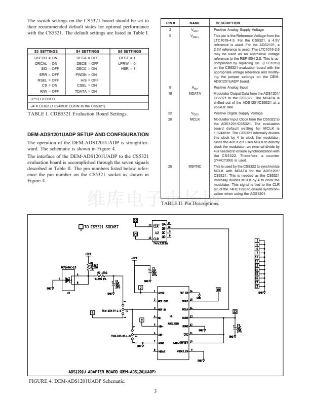
filter. The theory of operation and device specifications can
be found in the individual data sheets for these parts.
Martin Company, using the CS5321 evaluation board. The
鈭單?/div>
modulator with the CS5322
digital filter. The CS5321 accepts an analog input and
outputs a high-rate, low-resolution bit-stream to the CS5322
digital filter. The result from the digital filter is a low-rate,
high resolution (24-bit) digital representation of the analog
value. Since the basic operation of the ADS1201 and CS5321
is the same, the ADS1201 modulator can be used with the
CS5322 filter to obtain the same 24-bit digital representa-
tion. The following paragraph is an overview of how the
CS5321 evaluation board was setup to accommodate both
the ADS1201 and the CS5321.
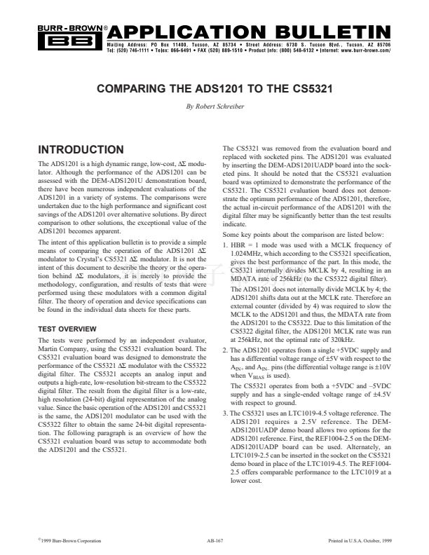
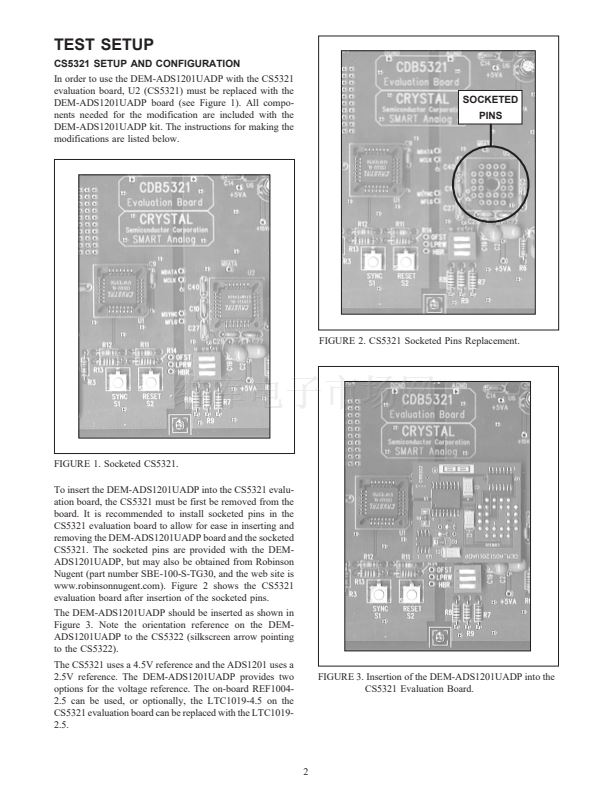
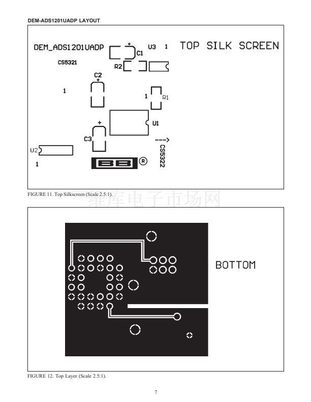
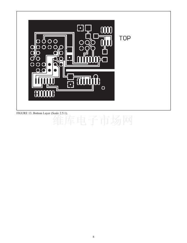
The CS5321 was removed from the evaluation board and
replaced with socketed pins. The ADS1201 was evaluated
by inserting the DEM-ADS1201UADP board into the sock-
eted pins. It should be noted that the CS5321 evaluation
board was optimized to demonstrate the performance of the
CS5321. The CS5321 evaluation board does not demon-
strate the optimum performance of the ADS1201, therefore,
the actual in-circuit performance of the ADS1201 with the
digital filter may be significantly better than the test results
indicate.
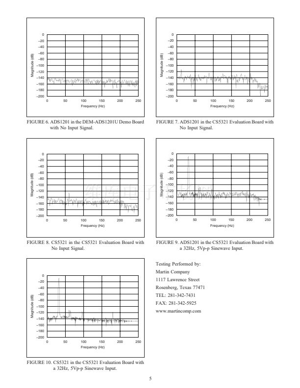
Some key points about the comparison are listed below:
1. HBR = 1 mode was used with a MCLK frequency of
1.024MHz, which according to the CS5321 specification,
gives the best performance of the part. In this mode, the
CS5321 internally divides MCLK by 4, resulting in an
MDATA rate of 256kHz (to the CS5322 digital filter).
The ADS1201 does not internally divide MCLK by 4; the
ADS1201 shifts data out at the MCLK rate. Therefore an
external counter (divided by 4) was required to slow the
MCLK to the ADS1201 and thus, the MDATA rate from
the ADS1201 to the CS5322. Due to this limitation of the
CS5322 digital filter, the ADS1201 MCLK rate was run
at 256kHz, not the optimal rate of 320kHz.
2. The ADS1201 operates from a single +5VDC supply and
has a differential voltage range of
鹵5V
with respect to the
A
IN+
and A
IN鈥?/div>
pins (the differential voltage range is
鹵10V
when V
BIAS
is used).
The CS5321 operates from both a +5VDC and 鈥?VDC
supply and has a single-ended voltage range of
鹵4.5V
with respect to ground.
3. The CS5321 uses an LTC1019-4.5 voltage reference. The
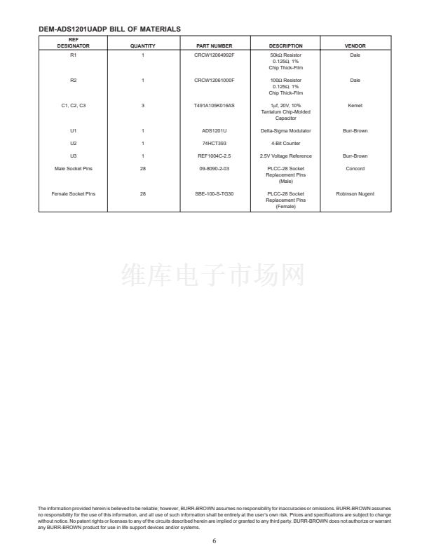
ADS1201 requires a 2.5V reference. The DEM-
ADS1201UADP demo board allows two options for the
ADS1201 reference. First, the REF1004-2.5 on the DEM-
ADS1201UADP board can be used. Alternately, an
LTC1019-2.5 can be inserted in the socket on the CS5321
demo board in place of the LTC1019-4.5. The REF1004-
2.5 offers comparable performance to the LTC1019 at a
lower cost.
漏
1999 Burr-Brown Corporation
AB-167
Printed in U.S.A. October, 1999


 1
1
 2
2
 3
3
 4
4
 5
5
 6
6
 7
7
 8
8
