廬
USING THE ADS1201 EVALUATION BOARD
By Saeid Jannesari
FEATURES
q
EASY INSTALLATION AND USE
q
ON BOARD
SINC
3
DIGITAL FILTER WITH PRO-
GRAMMABLE MODULATOR CLOCK AND DECI-
MATION RATIO
q
RETRIEVES FILTER OUTPUT DATA INTO PC
FOR ANALYSIS AND DISPLAY
q
PERFORMS FOURIER TRANSFORMS ON COL-
LECTED DATA
q
DISPLAYS DATA IN BOTH FREQUENCY AND
TIME DOMAIN
q
USER-FRIENDLY VISUAL BASIC鈩?GRAPHICAL
INTERFACE
This application bulletin provides information on the opera-
tion and usage of the ADS1201U evaluation fixture and
provides detailed description of the digital filter design
implemented into Xilinx XC4010E Field Programmable
Gate Array (FPGA). The latest information, along with the
FPGA files can be found on the Burr-Brown web site. The
ADS1201U evaluation board communicates to a PC via a bi-
directional parallel port. It is capable of collecting up to
8192 data words at a maximum data rate of 1000Hz. The
user interface software is written in Visual Basic and con-
trols the filter configuration and data retrieval, as well as
graphical display and analysis. Data can be displayed in time
and frequency domain. Optionally, retrieved data can be
saved to a file for transport to other graphical and math-
ematical software applications. In addition, a hard copy of
the displayed graphics in time or frequency domain can be
obtained. In this bulletin, a complete description of the
hardware and software features of the ADS1201U evalua-
tion kit will be given.
ADS1201U
Since the information in this bulletin concerns the
ADS1201U, the following is a brief description of the part.
ADS1201U is a single channel precision, wide dynamic
range, second-order Delta-Sigma (鈭單? modulator operating
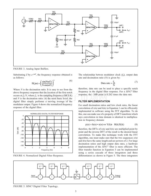
from a single +5V supply (see Figure 1 for device pinout).
The
鈭單?/div>
modulator converts an analog signal into a 1-bit
digital data stream of ones and zeros. The ones density of the
output data stream is proportional to the input analog signal.
Oversampling and noise shaping are used to reduce the
quantization noise in the frequency band of interest. A
鈭單?/div>
modulator can be used with a digital filter for wide dynamic
range A/D conversion of 24 bits of resolution or better.
Filtering the noise is the primary purpose of the digital filter.
Its secondary purpose is to convert the 1-bit data stream at
high sample rate into a higher bit data stream at lower rate
(decimation). The output data from the ADS1201U modula-
tor is read via the MOUT pin. The modulator outputs data at
the rising edge of MCLK with a short time delay, t
d
. It is
recommended to synchronize the reading of the output data
with the falling edge of MCLK (Figure 2). The collected
output of the modulator is then passed through a digital low-
pass filter and the resulting output word is decimated and
truncated to the desired data rate and effective resolution,
respectively. The combination of the
鈭單?/div>
modulator and the
digital decimation filter forms a
鈭單?/div>
A/D converter. For more
detailed information and specifications concerning the
ADS1201U modulator, refer to the ADS1201 data sheet.
AV
DD
REF
OUT
REF
IN
NIC
A
IN
P
A
IN
N
AGND
V
BIAS
1
2
3
4
ADS1201
5
6
7
8
16 REF
EN
15 MOUT
14 MCLK
13 DV
DD
12 DGND
11 CAL
10 GAIN/OFFSET
9
BIAS
EN
NIC: Not Internally Connected
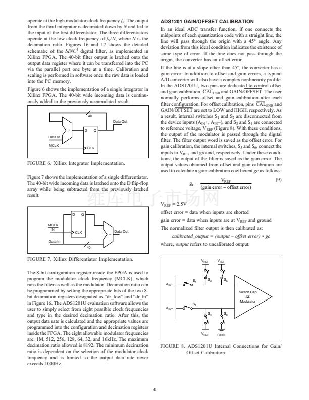
FIGURE 1. ADS1201U Device Pinout.
t
d
M
OUT
M
CLK
FIGURE 2. ADS1201U Output Read Operation.
The information provided herein is believed to be reliable; however, BURR-BROWN assumes no responsibility for inaccuracies or omissions. BURR-BROWN assumes
no responsibility for the use of this information, and all use of such information shall be entirely at the user鈥檚 own risk. Prices and specifications are subject to change
without notice. No patent rights or licenses to any of the circuits described herein are implied or granted to any third party. BURR-BROWN does not authorize or warrant
any BURR-BROWN product for use in life support devices and/or systems.
漏
1999 Burr-Brown Corporation
AB-146
Printed in U.S.A. May, 1999


 1
1
 2
2
 3
3
 4
4
 5
5
 6
6
 7
7
 8
8
 9
9
 10
10
 11
11
 12
12
 13
13
 14
14
