廬
OVERDRIVING THE INPUTS TO THE
ADS1210, ADS1211, ADS1212, AND ADS1213
By Bonnie C. Baker
1
A common situation, yet undesirable condition, is to have
the input signal of an A/D converter (such as one of Burr-
Brown鈥檚 delta-sigma converters) overdrive the input stage.
A possible question that arises in this situation is 鈥淲hat will
the output digital code become if the analog input is
overdriven?鈥?The differential analog input range of the
ADS1210, ADS1211, ADS1212 and ADS1213 analog-to-
digital converters, shown in Figure 1, can be configured to
operate in a unipolar or bipolar mode. In the unipolar mode,
the input range is generally 5Vp-p. For bipolar operation the
input range is generally 10Vp-p. This is true if the PGA
(internal Programmable Gain Amplifier) is programmed to
be 1, V
REF
= 2.5V, and a system calibration has not been
performed. In this discussion, the differential input voltage
is defined as V
INP
鈥揤
INM
, where V
INP
is defined as the
voltage at the non-inverting input (A
IN
P or A
IN
XP) of the
differential stage and V
INM
is defined as the voltage on the
inverting input (A
IN
N or A
IN
XN) with relation to ground.
Regardless of this definition of the input voltage range of the
converter, the actual acceptable input voltage limits of these
devices is 0 to 5V (this discussion assumes that V
DD
= 5V
and ground is defined as zero volts).
If either input exceeds these voltage values, the protection
circuitry will be enabled. Every pin of these
鈭單?/div>
converters
are ESD protected with the Burr-Brown鈥檚 standard ESD
protection cells shown in Figure 2. In the event of over
voltage stress on the input pins, the ESD devices will
forward bias. The product data sheets for these A/D convert-
ers recommend that the maximum and minimum limits of 0
to 5V on the inputs to the A/D converter not be exceeded by
more than 0.3V. Conversely, the device inputs will also
survive input or output currents of
鹵10mA,
continuous.
These restrictions are limited to continuous operation and
are exclusive of the situation where electrostatic charge is
momentarily injected into or out of these pins. In this
instance, the ESD protection diodes are designed to accept
these large, short spurts of energy and dissipate the heat
quickly. The ADS1210, ADS1211, ADS1212, and ADS1213
have been tested and passed to human body and machine
models.
Excluding ESD conditions, the case is examined where the
鈭單?/div>
A/D converter is being used under normal conditions
(meaning non-ESD conditions) and the input of the device is
3
4
AGND AV
DD
REF
OUT
REF
IN
V
BIAS
X
IN
X
OUT
MODE
A
IN
1P
A
IN
1N
A
IN
2P
A
IN
2N
A
IN
3P
A
IN
3N
A
IN
4P
A
IN
4N
MUX
A
IN
P
+2.5V
Reference
+3.3V Bias
Generator
Clock Generator
DGND
DV
DD
Micro Controller
Second-Order
鈭嗏垜
Modulator
Third-Order
Digital Filter
Instruction Register
Command Register
Data Output Register
Offset Register
Full-Scale Register
SCLK
SDIO
SDOUT
PGA
A
IN
N
Modulator Control
Serial Interface
ADS1211, ADS1213 Only
ADS1210/11
ADS1212/13
DSYNC
CS
DRDY
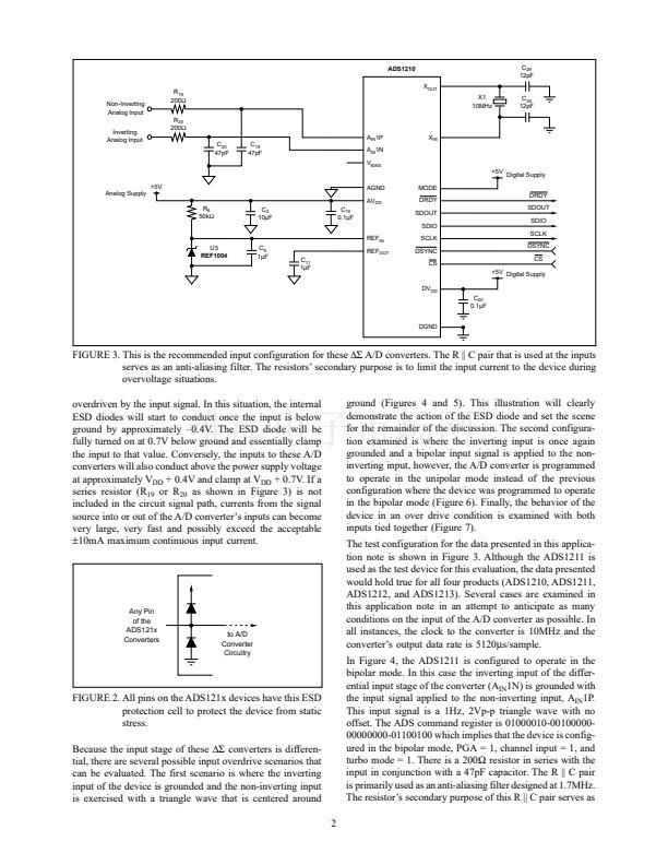
FIGURE 1. The ADS1210 and ADS1212 have one differential input to the device. The ADS1211 and ADS1213 have four
differential inputs that are internally multiplexed to the single A/D converter in the chips.
漏
1997 Burr-Brown Corporation
AB-115A
1
Printed in U.S.A. August, 1997


 1
1
 2
2
 3
3
 4
4
