multi-bit approach. The state-of-the-art
鈭單?/div>
converter contains a
programmable gain amplifier (PGA), a multi-order charge-
漏
1
balancing A/D converter, a calibration
碌C
with on-chip static
RAM, a clock oscillator, a programmable digital filter, and a bi-
directional serial communications port. The function of the
multi-order charge-balancing A/D converter can be conceptual-
ized with the first-order stage shown in the insert in Figure 1.
The analog input voltage and the output of the 1-bit DAC is
differentiated, providing an analog voltage at X
2
. The voltage at
X
2
is presented to the integrator. The output of the integrator
progresses in a negative or positive direction. The slope and
direction of the signal at X
3
is dependant on the sign and
magnitude of X
2
. At the time the voltage at X
3
equals the
comparator reference voltage, the output of the comparator
switches from negative to positive or positive to negative,
dependent on its original state. The output value of the com-
parator (X
4
) is clocked into the 1-bit DAC, as well as clocked
into the digital filter stage. At the time that the output of the
comparator switches from a HIGH to a LOW or visa versa, the
1-bit DAC responds on the next clock pulse by changing its
analog output voltage to the difference amplifier. This creates
a different output voltage at X
2
, causing the integrator to
progress in the opposite direction.
Analog
Input
PGA
1-Bit Data
Stream
Multi-Order
Charge-Balancing
A/D Converter
Digital
Low-Pass
Filter
Multi-Bit
Data
Decimation
Filter
Multi-Bit
Output Data
3
4
5
6
1st-Order Modulator
Difference Integrator Comparator
(1-Bit ADC)
Amp
X
3
X
2
鈭?/div>
X
4
Analog
Input
X
5
1-Bit DAC
FIGURE 1. A Block Diagram of a Generic
鈭單?/div>
A/D Converter.
Typically, this class of modulator has an input Programmable Gain
Amplifier that conditions the analog input signal. The PGA stage is
followed by the multi-order charge-balancing section which per-
forms the first step in low frequency noise reduction and digitizes the
signal into a stream of ones and zeros. This stage is followed by a
digital low pass filter and finally, a decimation stage. The digital low-
pass filter and decimation filter can be combined in some A/D
converters, dependent on the design topology used.
Printed in U.S.A. August, 1997
1996 Burr-Brown Corporation
AB-106A


 1
1
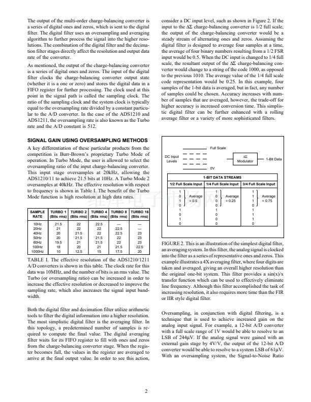 2
2
 3
3
 4
4
 5
5
 6
6
