廬
APPLICATION BULLETIN
By Uwe V枚hringer, Burr-Brown International GmbH
Mailing Address: PO Box 11400 鈥?Tucson, AZ 85734 鈥?Street Address: 6730 S. Tucson Blvd. 鈥?Tucson, AZ 85706
Tel: (520) 746-1111 鈥?Twx: 910-952-111 鈥?Telex: 066-6491 鈥?FAX (520) 889-1510 鈥?Immediate Product Info: (800) 548-6132
COMBINING AN AMPLIFIER WITH THE BUF634
COMBINED OP AMP AND BUFFER ACHIEVE
HIGHER OUTPUT POWER AND MORE SPEED
As long as amplifiers have existed, engineers have been
dreaming of an 鈥渋deal鈥?op amp. As little noise as possible,
high bandwidth, great precision, unlimited input impedance,
and output impedance close to 0鈩︹€攖hese are specifications
desirable for every application. Unfortunately, no op amp
can fulfill all of these requirements, particularly not while
remaining affordable. A good solution, therefore, is to com-
bine two components, using the best of both parts to achieve
desired specifications.
The following application note describes a combination
using an op amp with the high-speed buffer BUF634 located
in its feedback loop (see Figure 1). Depending upon the op
amp selected, large signals with output currents of over
500mA into the MHz range can be attained.
Possible applications for this combination include cable
drivers, virtual ground drivers for a dynamic load, or low
distortion end stages for both audio and video signal genera-
tors. In this circuit configuration, the work is divided so that
the op amp is responsible for precision while the buffer
provides the necessary current. An important advantage of
the combination is that the power dissipation is managed by
the buffer. The op amp is loaded only by the low input
current of the buffer amplifier. The temperature at the op
amp is only slightly higher than in the no-load mode. The
circuit parameters such as offset, drift, noise, and harmonic
distortion depend almost entirely upon the op amp used in
the circuit and have practically no influence on the configu-
ration even when the temperature of the buffer rises. The
combination was tested using four different op amps. The
measurement diagrams in Figures 3 through 15 show the
performance of the various combinations.
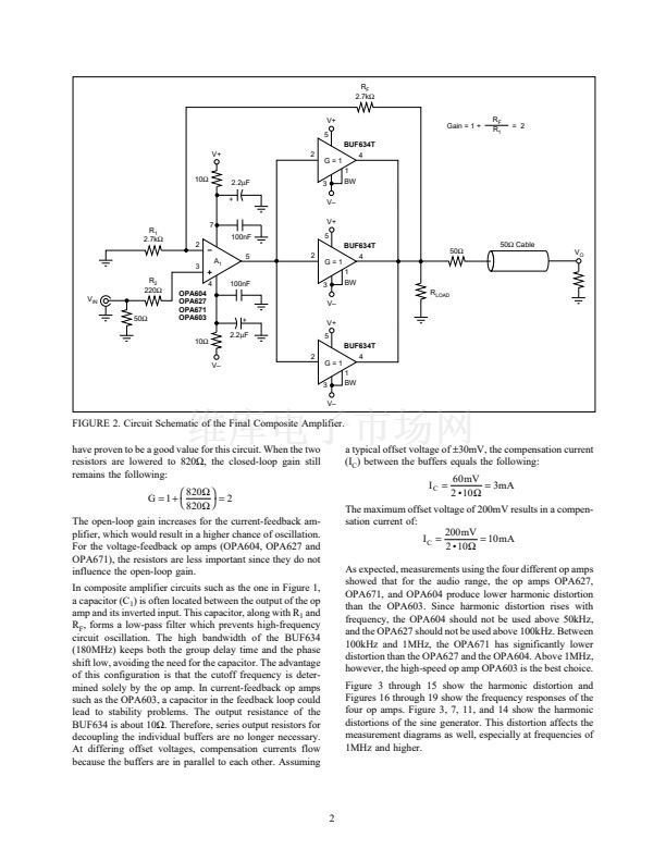
For low-end audio circuits, the OPA604 is used for low-
noise and low-distortion applications at frequencies of up to
about 100kHz. The OPA627, OPA671, and OPA603 are
used for higher frequency applications. As already men-
tioned, the buffer is located in the feedback loop of the op
amp. This configuration compensates the buffer鈥檚 internal
resistance so that the output resistance of the entire circuit is
close to zero. At high frequencies with high loads, however,
the internal resistance of the buffer increases, leading to a
rise in distortion as well. For this reason, the circuit contains
three BUF634T in parallel in order to achieve an output
current of 500mA, even though two of these components
would have sufficed for this current to be attained (see
Figure 2).
漏
V+
C
1
OPA
V
IN
BUF634
BW
V
O
V鈥?/div>
FIGURE 1. Composite Amplifier Using BUF634.
CALCULATING THE LOAD RESISTANCE (R
LOAD
)
FOR A 500mA OUTPUT CURRENT
The output voltage of the buffer was fixed at 15Vp-p for all
measurements to ensure that the op amp would remain
within its linear operating range. The circuit was configured
at gain 2 since the input is terminated at 50鈩?for the high
frequency measurements. To achieve the 15Vp-p output
voltage at gain 2, the following rms-input voltage is re-
quired:
V
IN
=
V
OUT
P鈭扨
2 鈥?2 鈥?Gain
=
15Vp鈭抪
=
2.652Vrms
2鈥?2 鈥?
The load resistance for a peak output current of 500mA
equals:
15Vp鈭抪
=
15鈩?/div>
2 鈥?500mA
The 50鈩?series resistor at the buffer outputs provides reflec-
tion-free termination in the high-frequency range. No series
resistors were used between the output of op amp A
1
and the
buffer inputs since they would form a low-pass filter in
combination with the input capacitance of the buffers. Any
phase shift resulting from this low-pass could cause the
entire circuit to oscillate, particularly when an op amp like
the OPA603 is used.
When selecting the value of resistors R
F
and R
1
, which
determine the gain, it should be noted that R
F
determines the
bandwidth and stability for current-feedback op amps, they
also determine the open-loop gain. Resistor values of 2.7k鈩?/div>
AB-101
Printed in U.S.A. September, 1995
1995 Burr-Brown Corporation


 1
1
 2
2
 3
3
 4
4
 5
5
 6
6
