廬
APPLICATION BULLETIN
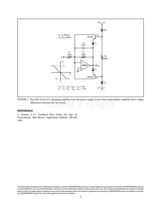
CLAMPING AMPLIFIER
TRACKS POWER SUPPLIES
By Jerald Graeme (602) 746-7412
Mailing Address: PO Box 11400 鈥?Tucson, AZ 85734 鈥?Street Address: 6730 S. Tucson Blvd. 鈥?Tucson, AZ 85706
Tel: (602) 746-1111 鈥?Twx: 910-952-111 鈥?Telex: 066-6491 鈥?FAX (602) 889-1510 鈥?Immediate Product Info: (800) 548-6132
Clamping amplifiers limit signal magnitude to protect fol-
lowing circuitry from input overload. The clamping ampli-
fier shown here produces limit levels that track the power
supply levels selected in any given test configuration. Con-
ventional clamping amplifiers set limit levels referenced to
ground, rather than the supply levels, and restrict signal
swing to the minimum available under minimum supply
conditions. However, the clamping amplifier shown auto-
matically adapts the clamp levels to supply changes, maxi-
mizing the allowable signal swing.
Traditional clamping amplifiers produce output voltage lim-
its referenced to common. However, the input overload
levels of most circuits depend upon voltage levels refer-
enced to the power supplies. There, the internal bias voltage
requirements of a circuit define minimum voltage separa-
tions between the signal and the power supply levels. This
references the overload levels to the supplies, rather than to
ground. Ground-referenced limits adequately accommodate
these bias requirements where the power supply levels
remain relatively fixed. Then, ground-referenced limits sim-
ply subtract fixed amounts from the worst-case, low supply
levels.
However, power supply levels vary greatly in test systems
where control signals set the supply levels. Then, the worst-
case setting of ground-referenced limits often sacrifices
operation in otherwise safe signal ranges. The clamping
amplifier shown adapts to supply variations by referencing
the clamp trip points to the supplies rather than to ground.
Higher supply voltages then produce higher clamp levels.
This avoids lost signal range by adapting the clamping limits
to the varying supply versus input capabilities of the follow-
ing circuit.
Basically, the circuit shown consists of an inverting ampli-
fier formed with the op amp, R
1
and R
2
. The remaining
components produce the clamping action, provide break-
down protection, and phase compensate the circuit. The
zener diodes, transistors and R
3
establish the basic clamp
reference voltages. Diodes D
1
and D
2
protect the transistors
from emitter-base breakdown and the capacitor compensates
the feedback stability complicated by the clamp. The circuit
clamps output e
O
by diverting feedback current away from
R
2
. This occurs when e
O
reaches a level sufficient to turn on
either Q
1
or Q
2
. Then, a transistor collector current absorbs
any additional signal current supplied through R
1
. No further
signal current reaches R
2
and this limits the level of e
O
.
Zener diodes D
Z1
and D
Z2
primarily determine the power
supply and clamp level relationships. These zeners establish
voltage levels with fixed separations from the supply volt-
ages. Diode D
Z1
biases the base of Q
1
at V
鈥?/div>
+V
Z1
, and D
Z2
sets
the base of Q
2
at V
+
鈥揤
Z2
. These base biases set the clamp
transistors for turn on at specific clamp levels. A negative
going e
O
turns on transistor Q
1
when e
O
reaches a level of V
L鈥?/div>
= V
鈥?/div>
+V
Z1
鈥?V
BE1
鈥?V
D1
. Then, Q
1
conducts current through
its collector, diverting any additional feedback current away
from R
2
. Any further increase in e
i
magnitude simply sup-
plies more current to Q
1
rather than to R
2
. This holds the
circuit output voltage at the turn-on level V
L鈥?/div>
. Similarly, a
positive going e
O
turns on Q
2
when e
O
reaches the positive
limit of V
L+
= V
+
鈥?V
Z2
+ V
BE2
+ V
D2
.
With the components shown, V
Z
= 6.2V and V
BE
and V
D
=
0.6V producing 10V output limiting for 15V supplies. Tol-
erance variations in the component voltages introduce a
400mV worst-case error to the clamp voltages. No signifi-
cant clamp-level error results from the precision OPA77
shown.
However, the clamp circuit adds gain in the feedback loop,
compromising feedback stability. When one of the clamp
transistors conducts, it acts as a common-base transistor in
the feedback loop. This adds a gain of (R
1
|| R
2
)/R
E
to the
open-loop gain of the amplifier. Here, R
E
represents the
impedance of the transistor鈥檚 emitter circuit and this imped-
ance is quite low. The emitter circuit impedance includes the
dynamic emitter impedance of the transistor and the forward
impedance of the diode. Feedback analysis
1
shows that this
added gain shifts the net open-loop gain upward, exposing a
region of two-pole response roll off. Lower closed-loop
gains encounter this stability-compromising region. For those
cases, the capacitor shown rolls off the load impedance of
the common-base transistors, removing the added gain at
high frequencies.
漏
1993 Burr-Brown Corporation
AB-054
Printed in U.S.A. April, 1993


 1
1
 2
2
