5817
ADDRESSABLE
28-LINE DECODER/DRIVER
5817
ADDRESSABLE
28-LINE DECODER/DRIVER
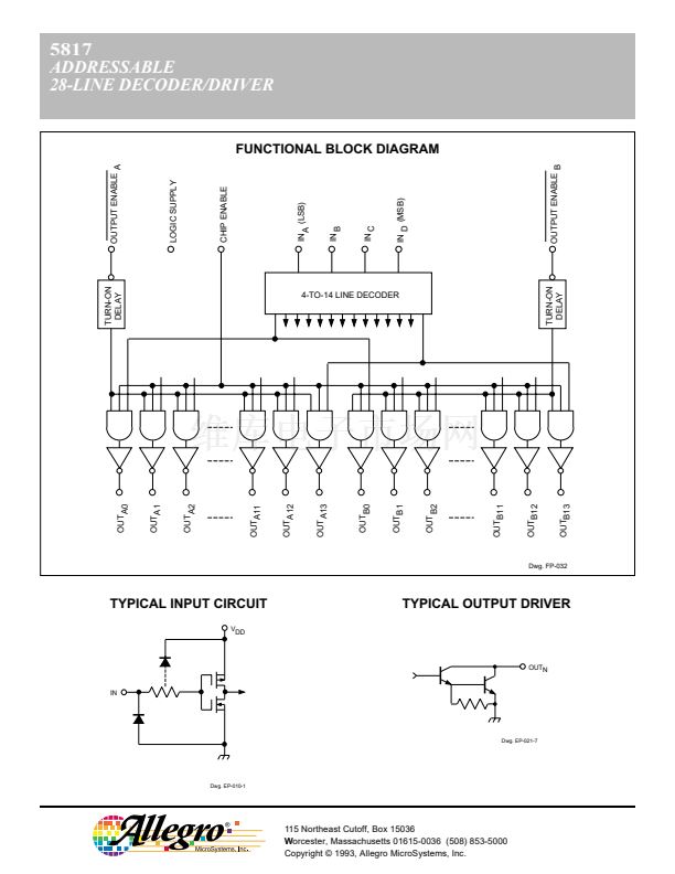
Intended for use in ink-jet printer applications, the A5817SEP
addressable 28-line decoder/driver combines low-power CMOS inputs
and logic with 28 high-current, high-voltage bipolar outputs. A 4-to-14
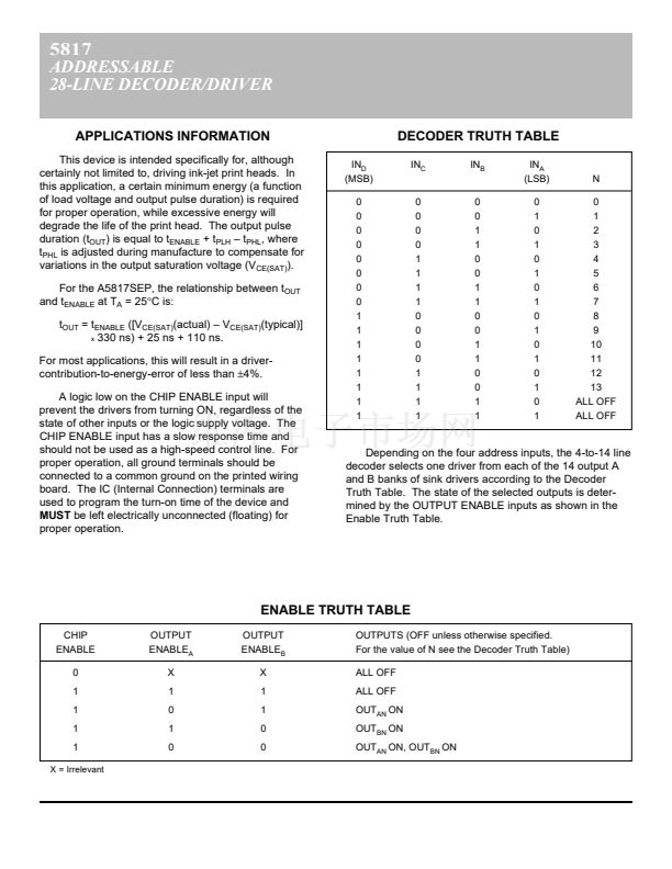
line decoder determines the selected output driver (n) in each
14-driver bank. Two independent output enable inputs (active low)
then provide the final decoding to activate 1- or 2-of-28 outputs
(OUT
An
and/or OUT
Bn
). Special internal circuitry is programmed at the
time of manufacture to adjust the output pulse timing and thereby the
energy the device delivers to the ink-jet print head.
The CMOS inputs cause minimal loading and are compatible with
standard CMOS, PMOS, and NMOS logic. Use with TTL or DTL
circuits may require appropriate pull-up resistors to ensure an input
logic high. The internal CMOS logic operates from a 5 V supply.
A CHIP ENABLE function is provided to lock out the drivers during
system power up. The 28 bipolar power outputs are open-collector
30 V Darlington drivers capable of sinking 500 mA at ambient
temperatures up to 85擄C.
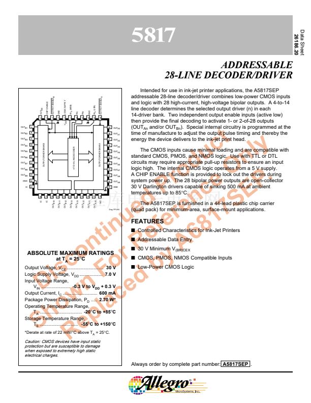
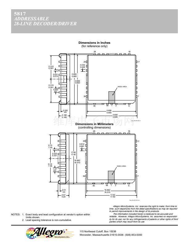
The A5817SEP is furnished in a 44-lead plastic chip carrier
(quad pack) for minimum-area, surface-mount applications.
Data Sheet
26186.20
OUTPUT ENABLE B
LOGIC SUPPLY
CHIP ENABLE
IN
D
(MSB)
GND
43
GND
IN
C
IN
B
42
41
IN
A
(LSB)
OUT B0
OUTB1
OUTB2
OUTB3
OUTB4
OUTB5
OUTB6
OUTB7
OUTB8
OUTB9
GND
IC
7
8
9
10
11
12
13
14
15
16
17
ABSOLUTE MAXIMUM RATINGS
at T
A
= 25
擄
C
Output Voltage, V
CE
.............................
30 V
Logic Supply Voltage, V
DD
..................
7.0 V
Input Voltage Range,
V
IN
.......................
-0.3 V to V
DD
+ 0.3 V
Output Current, I
C
...........................
600 mA
Package Power Dissipation, P
D
.....
2.70 W*
Operating Temperature Range,
T
A
.................................
-20
擄
C to +85
擄
C
Storage Temperature Range,
T
S
..............................
-55
擄
C to +150
擄
C
*Derate at rate of 22 mW/擄C above T
A
= 25擄C.
Caution: CMOS devices have input static
protection but are susceptible to damage
when exposed to extremely high static
electrical charges.
t y
c l
u n
d O .
o e P
r
P nc E
d e 7S
e r 1
u fe 8
in e 6
t R A
n r
o o
y
c F
b
s
i n
d
D
e
w lac
o p
h e
S R
39
38
37
36
35
34
33
32
31
OUTA0
OUTA1
OUTA2
OUTA3
OUTA4
OUTA5
OUTA6
OUTA7
OUTA8
OUTA9
GND
OUTPUT DRIVER BANK B
4-TO-14 LINE DECODER
OUTPUT DRIVER BANK A
V
DD
44
40
6
5
4
3
2
1
OUTPUT ENABLE A
30
29
25
19
20
18
21
22
23
24
OUTB11
OUTB10
OUTB13
OUTA11
A13
26
OUT
B12
OUTA12
A10
IC
IC
27
OUT
OUT
NC
28
Dwg. PP-050
FEATURES
s
Controlled Characteristics for Ink-Jet Printers
s
Addressable Data Entry
s
30 V Minimum V
(BR)CEX
s
CMOS, PMOS, NMOS Compatible Inputs
s
Low-Power CMOS Logic
Always order by complete part number:
A5817SEP
.


 1
1
 2
2
 3
3
 4
4
 5
5
 6
6
