SN75C1406
TRIPLE LOW-POWER DRIVERS/RECEIVERS
SLLS148D 鈥?MAY 1990 鈥?REVISED DECEMBER 1999
D
D
D
D
D
D
D
D
D
Meet or Exceed the Requirements of
TIA/EIA-232-F and ITU Recommendation
V.28
Very Low Power Consumption . . .
5 mW Typ
Wide Driver Supply Voltage Range . . .
鹵4.5
V to
鹵15
V
Driver Output Slew Rate Limited to
30 V/碌s Max
Receiver Input Hysteresis . . . 1000 mV Typ
Push-Pull Receiver Outputs
On-Chip Receiver 1-碌s Noise Filter
Functionally Interchangeable With Motorola
MC145406 and Texas Instruments
TL145406
Package Options Include Plastic
Small-Outline (D, DW, NS) Packages and
(N) DIPs
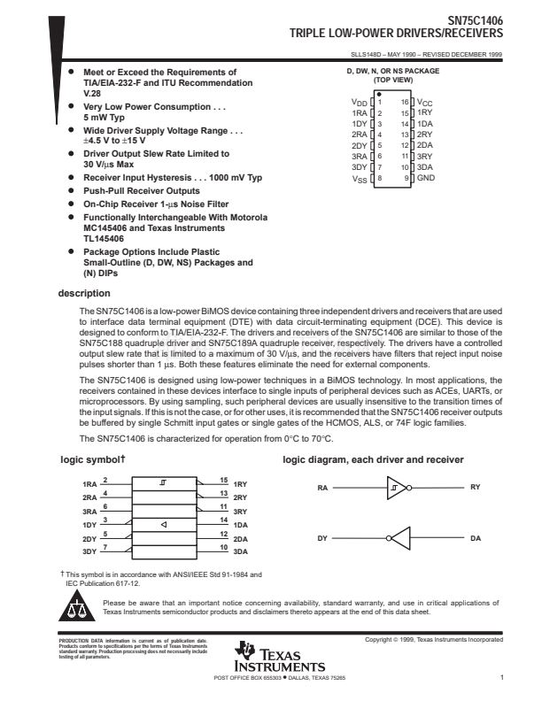
D, DW, N, OR NS PACKAGE
(TOP VIEW)
V
DD
1RA
1DY
2RA
2DY
3RA
3DY
V
SS
1
2
3
4
5
6
7
8
16
15
14
13
12
11
10
9
V
CC
1RY
1DA
2RY
2DA
3RY
3DA
GND
description
The SN75C1406 is a low-power BiMOS device containing three independent drivers and receivers that are used
to interface data terminal equipment (DTE) with data circuit-terminating equipment (DCE). This device is
designed to conform to TIA/EIA-232-F. The drivers and receivers of the SN75C1406 are similar to those of the
SN75C188 quadruple driver and SN75C189A quadruple receiver, respectively. The drivers have a controlled
output slew rate that is limited to a maximum of 30 V/碌s, and the receivers have filters that reject input noise
pulses shorter than 1
碌s.
Both these features eliminate the need for external components.
The SN75C1406 is designed using low-power techniques in a BiMOS technology. In most applications, the
receivers contained in these devices interface to single inputs of peripheral devices such as ACEs, UARTs, or
microprocessors. By using sampling, such peripheral devices are usually insensitive to the transition times of
the input signals. If this is not the case, or for other uses, it is recommended that the SN75C1406 receiver outputs
be buffered by single Schmitt input gates or single gates of the HCMOS, ALS, or 74F logic families.
The SN75C1406 is characterized for operation from 0擄C to 70擄C.
logic symbol
鈥?/div>
1RA
2RA
3RA
1DY
2DY
3DY
2
4
6
3
5
7
15
13
11
14
12
10
1RY
2RY
3RY
1DA
2DA
3DA
logic diagram, each driver and receiver
RA
RY
DY
DA
鈥?This symbol is in accordance with ANSI/IEEE Std 91-1984 and
IEC Publication 617-12.
Please be aware that an important notice concerning availability, standard warranty, and use in critical applications of
Texas Instruments semiconductor products and disclaimers thereto appears at the end of this data sheet.
PRODUCTION DATA information is current as of publication date.
Products conform to specifications per the terms of Texas Instruments
standard warranty. Production processing does not necessarily include
testing of all parameters.
Copyright
漏
1999, Texas Instruments Incorporated
POST OFFICE BOX 655303
鈥?/div>
DALLAS, TEXAS 75265
1


 1
1
 2
2
 3
3
 4
4
 5
5
 6
6
 7
7
 8
8
