74V2G66
DUAL BILATERAL SWITCH
s
s
s
s
s
s
HIGH SPEED:
t
PD
= 0.3ns (TYP.) at V
CC
= 5V
t
PD
= 0.4ns (TYP.) at V
CC
= 3.3V
LOW POWER DISSIPATION:
I
CC
= 1碌A(chǔ)(MAX.) at T
A
=25擄C
LOW 鈥漁N鈥?RESISTANCE:
R
ON
=6.5鈩?(TYP.) AT V
CC
= 5V I
I/O
= 1mA
R
ON
= 8.5鈩?(TYP.) AT V
CC
= 3.3V I
I/O
= 1mA
SINE WAVE DISTORTION:
0.04% AT V
CC
= 3.3V f = 1KHz
WIDE OPERATING RANGE:
V
CC
(OPR) = 2V TO 5.5V
IMPROVED LATCH-UP IMMUNITY
SOT23-8L
SOT323-8L
ORDER CODES
PACKAGE
SOT23-8L
SOT323-8L
T&R
74V2G66STR
74V2G66CTR
DESCRIPTION
The 74V2G66 is an advanced high-speed CMOS
DUAL BILATERAL SWITCH fabricated in silicon
gate C
2
MOS technology. It achieves high speed
propagation delay and VERY LOW ON
resistances while maintaining true CMOS low
power consumption. This bilateral switch handles
rail to rail analog and digital signals that may vary
across the full power supply range (from GND to
V
CC
)
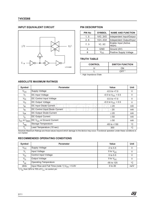
The C input is provided to control the switch and
it鈥檚 compatible with standard CMOS output; the
switch is ON (port I/O is connected to Port O/I)
when the C input is held high and OFF (high
impedance state exists between the two ports)
when C is held low. It can be used in many
application as Battery Powered System, Test
Equipment. It鈥檚 available in the commercial and
extended temperature range in SOT23-8L and
SC-70-8L package. All inputs and output are
equipped with protection circuits against static
discharge, giving them ESD immunity and
transient excess voltage.
PIN CONNECTION AND IEC LOGIC SYMBOLS
December 2001
1/11


 1
1
 2
2
 3
3
 4
4
 5
5
 6
6
 7
7
 8
8
 9
9
 10
10
 11
11
