鈮?/div>
t
PHL
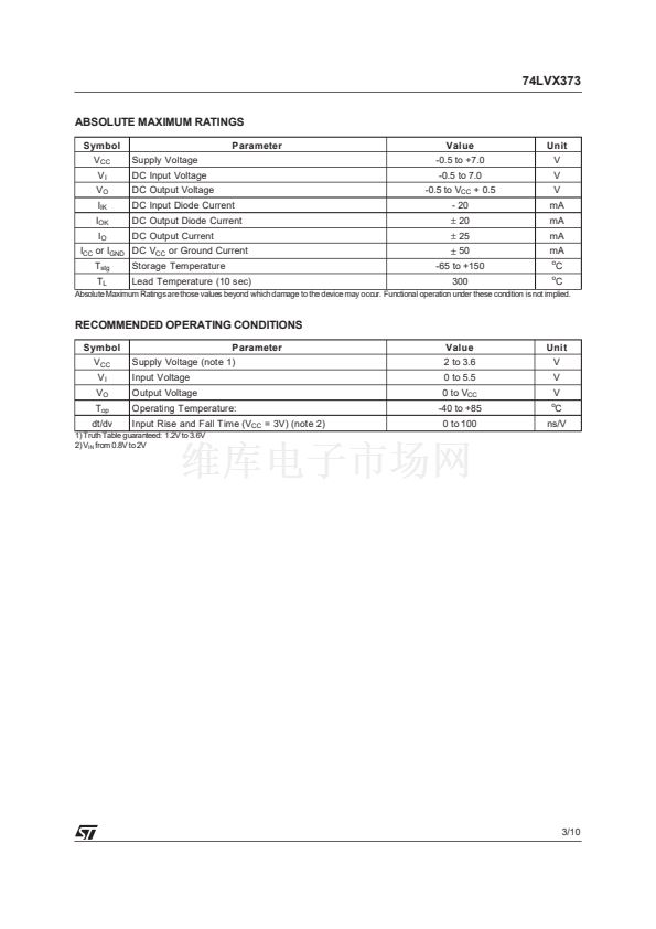
OPERATING VOLTAGE RANGE:
V
CC
(OPR) = 2V to 3.6V
PIN AND FUNCTION COMPATIBLE WITH
74 SERIES 373
IMPROVED LATCH-UP IMMUNITY
M
(Micro Package)
T
(TSSOP Package)
ORDER CODES :
74LVX373M
74LVX373T
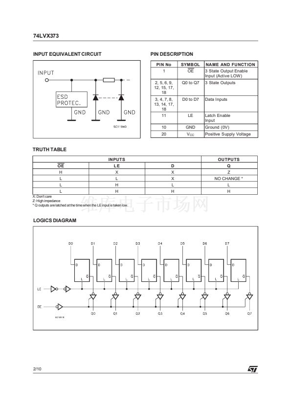
While the LE input is held at a high level, the Q
outputs will follow the data input precisely.
When the LE is taken low, the Q outputs will be
latched precisely at the logic level of D input data.
While the (OE) input is low, the 8 outputs will be
in a normal logic state (high or low logic level)
and while high level the outputs will be in a high
impedance state.
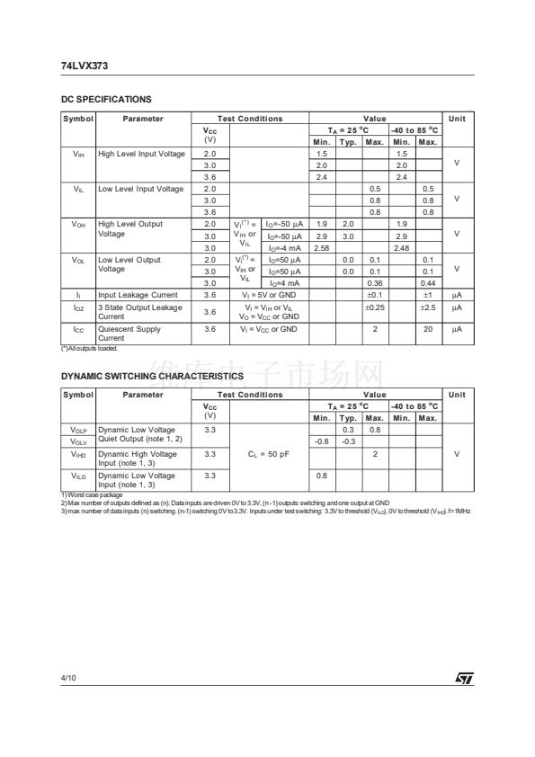
It has better speed performance at 3.3V than 5V
LS-TTL family combined with the true CMOS low
power consuption.
Power down protection is provided on all inputs
and 0 to 7V can be accepted on inputs with no
regard to the supply voltage. This device can be
used to interface 5V to 3V.
All inputs and outputs are equipped with
protection circuits against static discharge, giving
them 2KV ESD immunity and transient excess
voltage.
DESCRIPTION
The LVX373 is a low voltage CMOS OCTAL
D-TYPE LATCH with 3 STATE OUTPUT NON
INVERTING fabricated with sub-micron silicon
gate and double-layer metal wiring C
2
MOS
technology. It is ideal for low power and low noise
3.3V applications.
This 8 bit D-Type latch is controlled by a latch
enable input (LE) and an output enable input
(OE).
PIN CONNECTION AND IEC LOGIC SYMBOLS
May 1999
1/10


 1
1
 2
2
 3
3
 4
4
 5
5
 6
6
 7
7
 8
8
 9
9
 10
10
