鈮?/div>
t
PHL
OPERATING VOLTAGE RANGE:
V
CC
(OPR) = 2V to 3.6V (1.2V Data Retention)
PIN AND FUNCTION COMPATIBLE WITH
74 SERIES 125
IMPROVED LATCH-UP IMMUNITY
M
(Micro Package)
T
(TSSOP Package)
ORDER CODES :
74LVX125M
74LVX125T
This device requires the 3-STATE control input G
to be set high to place the output into the high
impedance state.
It has better speed performance at 3.3V than 5V
LS-TTL family combined with the true CMOS low
power consumption.
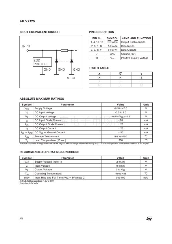
Power down protection is provided on all inputs
and 0 to 7V can be accepted on inputs with no
regard to the supply voltage. This device can be
used to interface 5V to 3V.
All inputs and outputs are equipped with
protection circuits against static discharge, giving
them 2KV ESD immunity and transient excess
voltage.
DESCRIPTION
The LVX125 is a low voltage CMOS QUAD BUS
BUFFERS fabricated with sub-micron silicon gate
and
double-layer metal
wiring
C
2
MOS
technology. It is ideal for low power and low noise
3.3V applications.
PIN CONNECTION AND IEC LOGIC SYMBOLS
April 1999
1/9


 1
1
 2
2
 3
3
 4
4
 5
5
 6
6
 7
7
 8
8
 9
9
