鈥?/div>
R
ON
t
4
W
Typical
Less Than 0.25 ns鈭扢ax Delay Through Switch
Nearly Zero Standby Current
No Circuit Bounce
Control Inputs are TTL/CMOS Compatible
Pin鈭扚or鈭扨in Compatible With QS3400, FST3400, CBT3400
All Popular Packages: SOIC鈭?4, TSSOP鈭?4, QSOP鈭?4
All Devices in Package TSSOP are Inherently Pb鈭扚ree*
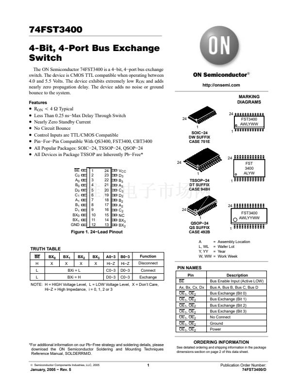
24
BE
C
0
A
0
B
0
D
0
C
1
A
1
B
1
D
1
BX
0
BX
1
GND
1
2
3
4
5
6
7
8
9
10
11
12
24
23
22
21
20
19
18
17
16
15
14
13
V
CC
D
3
B
3
A
3
C
3
D
2
B
2
A
2
C
2
NC
BX
3
BX
2
24
FST
3400
ALYW
1
1
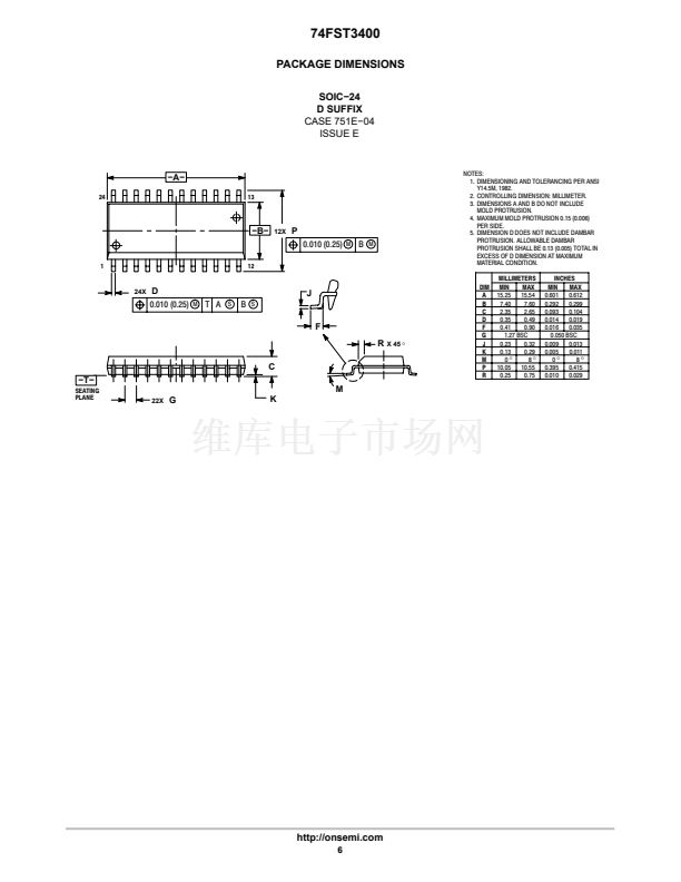
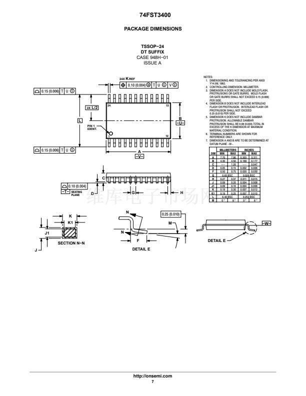
TSSOP鈭?4
DT SUFFIX
CASE 948H
24
24
1
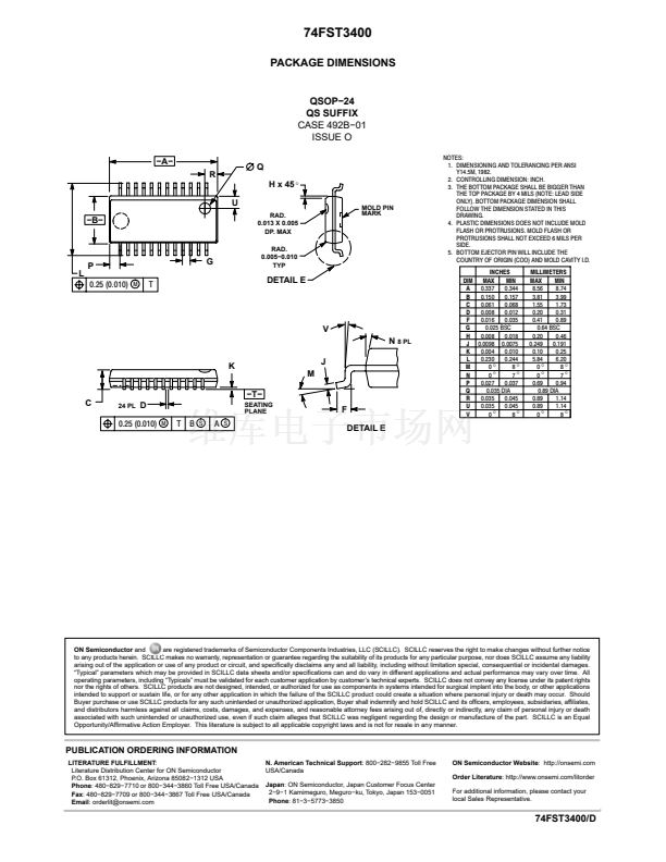
QSOP鈭?4
QS SUFFIX
CASE 492B
A
L, WL
Y, YY
W, WW
=
=
=
=
FST3400
AWLYYWW
1
Figure 1. 24鈭扡ead Pinout
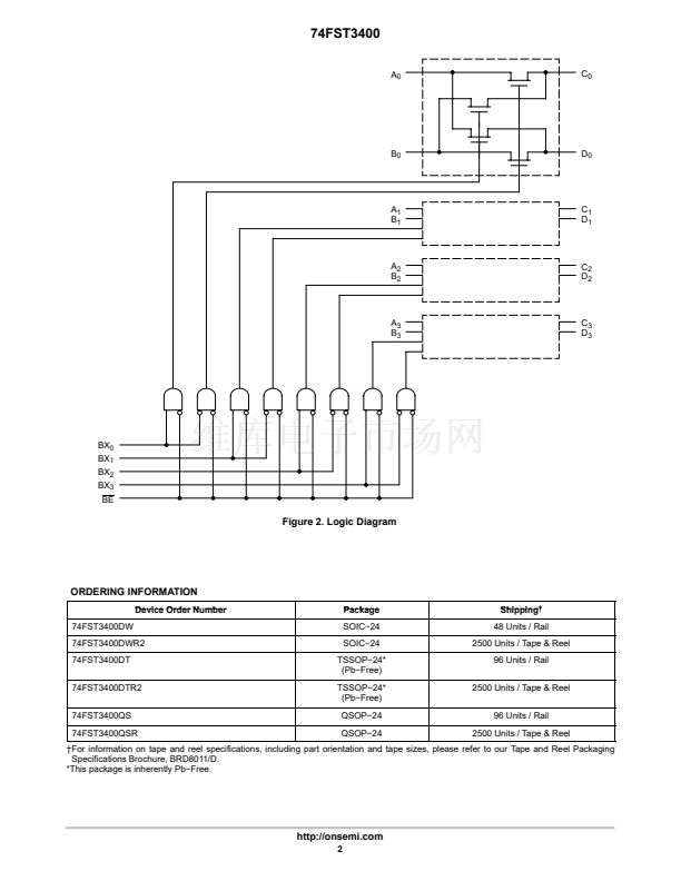
TRUTH TABLE
BE
H
L
L
BX
0
X
BX
1
X
BX
2
X
BXi = L
BXi = H
BX
3
X
A0鈭?
Hi鈭抁
C0鈭?
D0鈭?
B0鈭?
Hi鈭抁
D0鈭?
C0鈭?
Function
Disconnect
Connect
Exchange
BE
Assembly Location
Wafer Lot
Year
Work Week
PIN NAMES
Pin
Ax, Bx, Cx, Dx
OE
1
, OE
2
OE
1
, OE
2
OE
1
, OE
2
OE
1
, OE
2
OE
1
, OE
2
OE
1
, OE
2
OE
1
, OE
2
Description
Bus Enable Input (Active LOW)
Bus A, Bus B, Bus C, Bus D
Bus Exchange (Bit 0)
Bus Exchange (Bit 1)
Bus Exchange (Bit 2)
Bus Exchange (Bit 3)
No Connect
Ground
Power
NOTE: H = HIGH Voltage Level, L = LOW Voltage Level, X = Don鈥檛 Care,
NOTE:
Hi鈭抁 = High Impedance, i = 0, 1, 2 or 3
*For additional information on our Pb鈭扚ree strategy and soldering details, please
download the ON Semiconductor Soldering and Mounting Techniques
Reference Manual, SOLDERRM/D.
漏
Semiconductor Components Industries, LLC, 2005
ORDERING INFORMATION
See detailed ordering and shipping information in the package
dimensions section on page 2 of this data sheet.
1
January, 2005 鈭?Rev. 5
Publication Order Number:
74FST3400/D


 1
1
 2
2
 3
3
 4
4
 5
5
 6
6
 7
7
 8
8
