74F652 Transceivers/Registers
March 1988
Revised January 2004
74F652
Transceivers/Registers
General Description
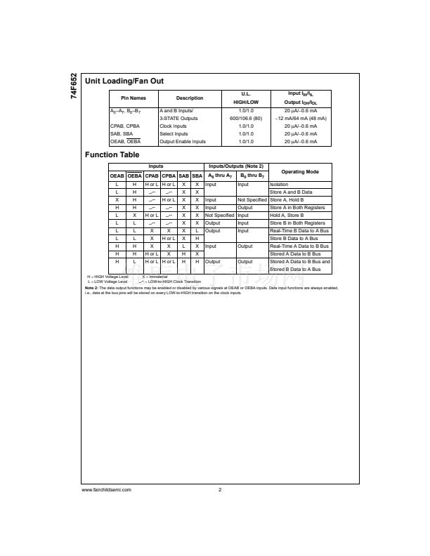
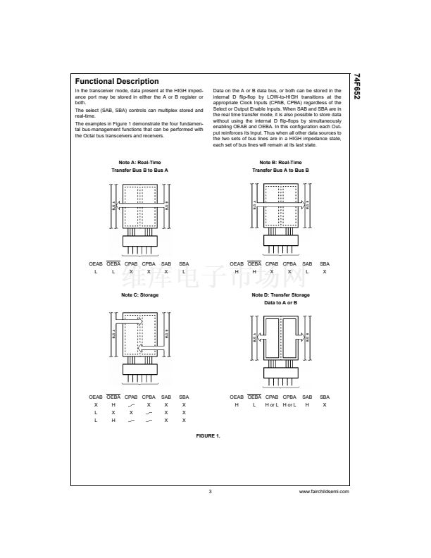
These devices consist of bus transceiver circuits with
D-type flip-flops, and control circuitry arranged for multi-
plexed transmission of data directly from the input bus or
from internal registers. Data on the A or B bus will be
clocked into the registers as the appropriate clock pin goes
to HIGH logic level. Output Enable pins (OEAB, OEBA) are
provided to control the transceiver function.
Features
s
Independent registers for A and B buses
s
Multiplexed real-time and stored data
s
74F652 non-inverting data path
Ordering Code:
Order Number
74F652SC
(Note 1)
74F652SPC
Package Number
M24B
N24C
Package Description
24-Lead Small Outline Integrated Circuit (SOIC), JEDEC MS-013, 0.300" Wide
24-Lead Plastic Dual-In-Line Package (PDIP), JEDEC MS-001, 0.300" Wide
Note 1:
Devices also available in Tape and Reel. Specify by appending the suffix letter 鈥淴鈥?to the ordering code.
Logic Symbols
Connection Diagram
IEEE/IEC
漏 2004 Fairchild Semiconductor Corporation
DS009581
www.fairchildsemi.com


 1
1
 2
2
 3
3
 4
4
 5
5
 6
6
 7
7
 8
8
