鈥?/div>
18鈥損in package
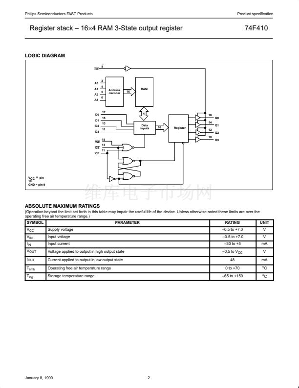
DESCRIPTION
The 74F410 is a register oriented high speed
64鈥揵it read/write memory organized as
16鈥搘ords by 4鈥揵its. An edge鈥搕riggered 4鈥揵it
output register allows new input data to be
written while previous data is held. 3鈥搒tate
outputs are provided for maximum versatility.
The 74F410 is fully compatible with all TTL
families.
TYPICAL
SUPPLY
CURRENT
( TOTAL)
45mA
while WE, CS, and CP are low, the contents
of the selected memory location follow these
changes provided setup and hold time criteria
are met.
Read operation
鈥?When CS is low, WE is
high, and CP goes from low鈥搕o鈥揾igh, the
contents of the memory location selected by
the address inputs (A0鈥揂3) are edge鈥?/div>
triggered into the output register.
When WE is low, CS is low, CP goes from
low鈥搕o鈥揾igh, the data at the data inputs is
edge鈥搕riggered into the output register. The
OE input controls the output buffers. When
OE is high the four outputs (Q0鈥換3) are in a
high impedance or off state; when OE is low,
the outputs are determined by the state of the
output register.
TYPE
74F410
TYPICAL
ACCESS
TIME
19.5ns
FUNCTIONAL DESCRIPTION
Write operation
鈥?When the three control
inputs, write enable (WE), chip select (CS),
and clock (CP), are low the information on
the data inputs (D0鈥揇3) is written into the
memory location selected by the address
inputs (A0鈥揂3). If the input data changes
ORDERING INFORMATION
ORDER CODE
DESCRIPTION
COMMERCIAL RANGE
V
CC
= 5V
鹵
10%, T
amb
= 0
擄
C to +70
擄
C
18鈥損in plastic DIP (300mil)
N74F410N
INPUT AND OUTPUT LOADING AND FAN OUT TABLE
PINS
D0 鈥?D3
A0 鈥?A3
CP
CS
OE
WE
Data inputs
Address inputs
Clock pulse input (active rising edge)
Chip select input (active low)
Output enable input (active low)
Write enable input (active low)
DESCRIPTION
74F (U.L.)
HIGH/LOW
1.0/1.0
1.0/1.0
1.0/2.0
1.0/2.0
1.0/1.0
1.0/1.0
150/40
LOAD VALUE
HIGH/LOW
20碌A(chǔ)/0.6mA
20碌A(chǔ)/0.6mA
20碌A(chǔ)/1.2mA
20碌A(chǔ)/1.2mA
20碌A(chǔ)/0.6mA
20碌A(chǔ)/0.6mA
3mA/24mA
Q0 鈥?Q3
Data outputs
NOTE:
One (1.0) FAST unit load is defined as: 20碌A(chǔ) in the high state and 0.6mA in the low state.
PIN CONFIGURATION
LOGIC SYMBOL
17 15 13 11
IEC/IEEE SYMBOL
3
4
5
6
2
1
7
1C
& G2
8
17
15
EN3
A1,2D
A3
16
14
12
10
0
A
1
&
G1
0
15
CS 1
WE 2
A0 3
A1 4
A2 5
A3 6
CP 7
OE 8
GND 9
18 V
CC
17 D0
16 Q0
15 D1
14 Q1
13 D2
12 Q2
11 D3
10 Q3
V
CC
= Pin 18
GND = Pin 9
16 14 12 10
3
4
5
6
1
2
7
8
A0
A1
A2
A3
CS
WE
CP
OE
Q0 Q1 Q2 Q3
D0 D1 D2 D3
13
11
January 8, 1990
1
853-1310 98498


 1
1
 2
2
 3
3
 4
4
 5
5
