74F299 Octal Universal Shift/Storage Register
April 1988
Revised August 1999
74F299
Octal Universal Shift/Storage Register
with Common Parallel I/O Pins
General Description
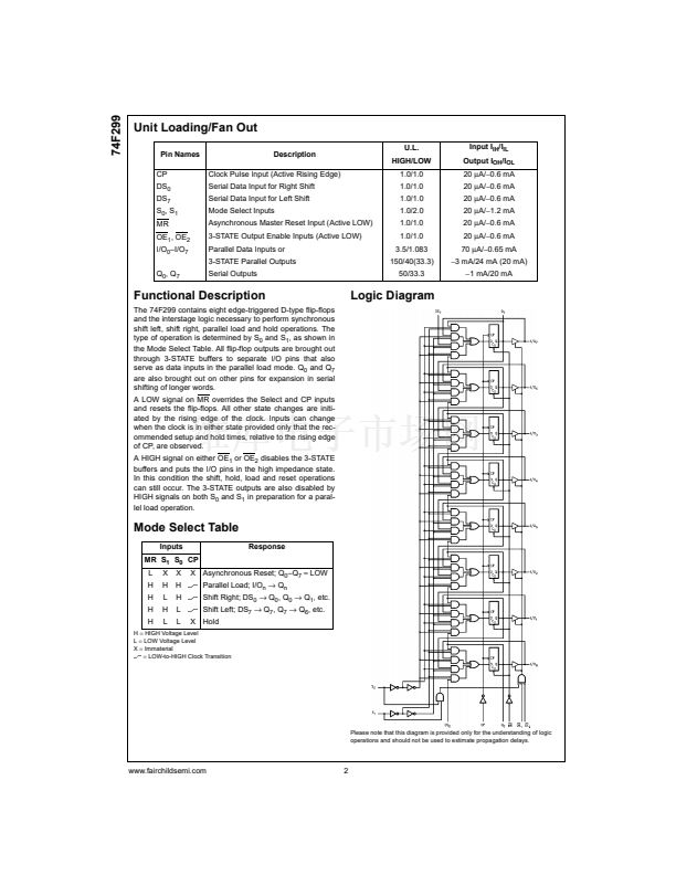
The 74F299 is an 8-bit universal shift/storage register with
3-STATE outputs. Four modes of operation are possible:
hold (store), shift left, shift right and load data. The parallel
load inputs and flip-flop outputs are multiplexed to reduce
the total number of package pins. Additional outputs, Q
0
鈥?/div>
Q
7
, are provided to allow easy serial cascading. A separate
active LOW Master Reset is used to reset the register.
Features
s
Common parallel I/O for reduced pin count
s
Additional serial inputs and outputs for expansion
s
Four operating modes: shift left, shift right, load and
store
s
3-STATE outputs for bus-oriented applications
s
Guaranteed 4000V minimum ESD protection
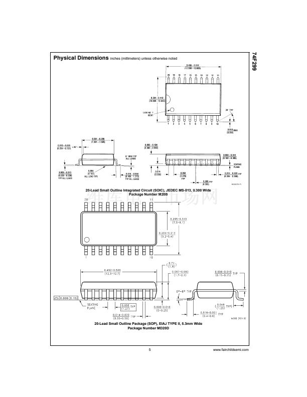
Ordering Code:
Order Number
74F299SC
74F299SJ
74F299PC
Package Number
M20B
M20D
N20A
Package Description
20-Lead Small Outline Integrated Circuit (SOIC), JEDEC MS-013, 0.300 Wide
20-Lead Small Outline Package (SOP), EIAJ TYPE II, 5.3mm Wide
20-Lead Plastic Dual-In-Line Package (PDIP), JEDEC MS-001, 0.300 Wide
Devices also available in Tape and Reel. Specify by appending the suffix letter 鈥淴鈥?to the ordering code.
Logic Symbols
Connection Diagram
IEEE/IEC
漏 1999 Fairchild Semiconductor Corporation
DS009515
www.fairchildsemi.com


 1
1
 2
2
 3
3
 4
4
 5
5
 6
6
